Author Archives: Erin

pcb-prototype

PCB Design Best Practices: Tips from the Experts

PCB Assembly service in Los AngelesPrinted Circuit Boards (PCBs) are the backbone of modern electronic devices. From smartphones to industrial machinery, PCBs ensure that electrical components are connected and function properly. Whether you’re developing a small prototype or scaling up production, good PCB design practices are critical to success. Here are some expert tips to help you design efficient, high-quality PCBs.

1. Plan Your Layout Strategically

The layout of your PCB can make or break your design. Start by organizing components based on their function and proximity to each other. Grouping similar components minimizes the length of signal paths, which helps reduce electromagnetic interference (EMI) and improves overall signal integrity. Additionally, ensure that your printed circuit boards have enough space to accommodate each component without overcrowding.

Visit our PCB Layout Services to learn how we can assist with optimizing your design layout.

2. Prioritize Signal Integrity

Signal integrity is essential to the reliable performance of your circuit. To maintain high signal quality, route sensitive traces such as clock signals away from high-current traces. Consider using differential pairs for high-speed signals to minimize noise. Proper grounding and shielding techniques can also help reduce noise and improve signal integrity.

Discover how our PCB Assembly Services can help ensure the highest levels of signal integrity in your projects.

3. Optimize Power Distribution

Power distribution is often overlooked but is crucial for maintaining the stability of your PCB. Design a robust power distribution network with ample decoupling capacitors placed near power pins to minimize voltage fluctuations. Use wide traces for power and ground planes to reduce resistance and ensure reliable power delivery.

Learn more about our PCB Power Distribution Solutions that can help you build a reliable power network for your design.

4. Minimize Crosstalk

Crosstalk occurs when signals on nearby traces interfere with each other, leading to performance issues or even complete system failure. To minimize crosstalk, increase the spacing between parallel signal traces or route them perpendicularly across different layers. You can also add ground planes between signal layers to shield traces from interference.

For more expert insights on reducing crosstalk, check out our PCB Expert Advice.

5. Use Design for Manufacturability (DFM) Principles

DFM ensures that your PCB design is optimized for easy and cost-effective manufacturing. This involves following industry standards for trace widths, hole sizes, and pad dimensions, as well as minimizing the use of unnecessary vias. Working closely with your manufacturer during the design phase will help avoid costly errors and delays later in production.

For expert guidance on DFM, contact our team at Board Assembly.

6. Test and Simulate Early and Often

Testing is a critical part of the PCB design process. Use simulation tools to verify the performance of your PCB design before manufacturing. Early testing helps identify potential issues such as signal interference, power integrity problems, or thermal issues, allowing you to make adjustments without incurring costly rework.

Check out our PCB Testing Services to learn more about how we ensure the reliability of your PCBs.

Printed Circuit Board FabricationFollowing these PCB design best practices can lead to more efficient, reliable, and manufacturable printed circuit boards. Whether you’re designing a simple prototype or a complex multi-layer PCB, keeping these tips in mind will help you achieve optimal results.
If you need expert support with your PCB design, assembly, or testing, visit Board Assembly and explore our wide range of services. We’re here to help you bring your designs to life with precision and quality.

Ready to get started? Contact our team at Board Assembly for professional PCB design and manufacturing support.

Flexible Circuit board

Flex Turnkey PCB Assembly

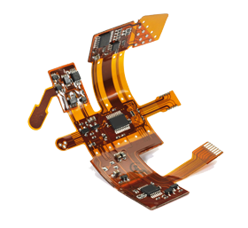
The design rules for flex turnkey PCB assembly is very similar to the design rules for traditional PCBs.  Traditional PCBs and flex flex turnkey PCB assembly share some similarities in the manufacturing process as well.  To start, the flexible circuit board material (typically copper clad Polyimide) is chosen, drilled, plated, photo-imaged, and imprinted just like the conservative PCB process. Next, both PCBs and flex turnkey PCB assemblies involve the panels being baked to remove any moisture from the wet processes.  This next step is where the original PCB and flex turnkey PCB assembly start to differ.  Flex turnkey PCB assemblies go to the cover lay station instead of going to the fuse mask station, as would occur with traditional PCBs.

A flex circuit board cover lay, also known as a cover film, is a lamination process used to summarize and protect any peripheral circuitry of the flex circuit. The cover lay serves the similar function as the solder mask does for conventional PCBs with the dissimilarity being the added component of flexibility. Naturally, the thickness of the cover lay is prepared of 1 mil thick Polyimide with a 1 mil thick, attach adhesive, but other thicknesses are accessible to meet precise design necessities. The Polyimide and adhesive cover lay is laminated using force and heat.

Flexible circuitThe heat allows for simple flow of the adhesive which is needed because it must fill-in any and all gaps among the traces and pads to stop the trapping of air between layers. To a flex turnkey PCB assembly designer this means the cover lay openings for a characteristic 1 oz. The copper plan must be out-sized by 10 mils, which is appreciably bigger than the typical huge of 2-3 mils used on conventional PCB solder masks.

ACME PCB Assembly manufactures flexible turnkey PCB assembly.  We can take your flexible circuit application from concept to reality with our complete design capabilities.  Our talented team is equipped to work in multiple data formats. We have in-house surface-mount technology (SMT) capabilities  and specialize in turnkey assembly applications.

ACME PCB Assembly will work with you for all of your flexible circuit board needs. We are committed to not only customer satisfaction, but exceeding our customer’s expectations. Our adherence to quality standards is a part of what makes our boards superior to other suppliers.

We provide a complete suite of PCB Assembly Services, including rework and modification, BGA, SMT, Turnkey, Thru-Hole, Lead Free, and Prototype assembly, plus an extensive line of add-on services, such as Injection Molding and Metal Work & Finishing.

Call us today with any questions 1- 310-715-1898  (Sales Extension 210) (Purchasing Extension 160)

Frequently Asked Question

What are the advantages of flexible turnkey PCB assembly over traditional printed circuit boards?

Flexible turnkey PCB assembly allows printed circuit boards to bend and fit into compact or uniquely shaped products without sacrificing performance. Flex PCBs reduce wiring, save space, improve durability, and are ideal for medical devices, automotive electronics, aerospace systems, industrial controls, and consumer electronics. ACME PCB Assembly provides complete flexible PCB design, fabrication, SMT assembly, prototype development, and turnkey manufacturing services to help bring your project from concept to production.

Printed Circuit Board Fabrication

Top Benefits of Using High-Quality PCBs in Your Projects

In today’s fast-paced technology landscape, using high-quality PCBs in your projects is essential for success. Printed circuit boards form the backbone of countless devices, from smartphones to industrial machines, and their performance can make or break your innovation. Ensuring that the printed circuit boards you select meet rigorous standards and are produced under stringent quality control measures is key to delivering reliable, durable, and efficient products.

Printed Circuit Board FabricationWhen working on any tech-driven project, it’s crucial to focus on the longevity and performance of your components. High-quality PCBs offer enhanced reliability, reducing the likelihood of malfunction or failure in the field. This is especially important in industries where downtime can result in costly delays or safety hazards. By sourcing printed circuit boards from a trusted provider like Board Assembly, you ensure that each PCB is meticulously inspected and tested, guaranteeing that it can withstand even the most challenging environments.

Another critical advantage of using high-quality PCBs is their ability to handle complex circuitry while maintaining efficiency. Whether your project involves compact devices or large-scale applications, well-designed printed circuit boards allow for optimal layout, minimizing noise and interference while maximizing performance. Quality control throughout the production process ensures that each board is built to precise specifications, eliminating errors and inconsistencies that could otherwise impact functionality.

Beyond functionality, investing in high-quality PCBs also enhances the overall reputation of your product. By delivering a reliable, robust solution to your customers, you establish trust and credibility, setting your business apart from competitors who may cut corners by using inferior components. The importance of partnering with a company like Board Assembly that prioritizes quality control cannot be overstated.

In conclusion, using high-quality PCBs in your projects isn’t just a technical requirement—it’s a strategic move to ensure long-term success and market differentiation. If you’re looking to integrate printed circuit boards that are built to last, perform reliably, and meet the highest standards, visit Board Assembly today to explore how their expertise and commitment to excellence can elevate your next project.

Frequently Asked Question

Why are high-quality printed circuit boards important for electronics manufacturing?

High-quality printed circuit boards improve reliability, electrical performance, and product lifespan while reducing the risk of manufacturing defects and costly failures. Partnering with Board Assembly ensures your PCBs are manufactured with strict quality control, advanced testing, and precision assembly. Learn more about our PCB assembly services and how we can help bring your next project to life.

PCB Fabrication and Assembly

Understanding the PCB Manufacturing Process: From Design to Production

PCB Fabrication near mePrinted Circuit Boards (PCBs) are the backbone of modern electronics, found in everything from smartphones to medical devices.

At Board Assembly, we pride ourselves on our comprehensive PCB manufacturing process, which ensures top-quality products for a wide range of industries. In this blog, we’ll walk you through the PCB manufacturing process, from initial design to the final product.

1. Design and Layout

The PCB manufacturing journey begins with the design phase. Engineers use specialized software to create a detailed layout of the circuit. This design includes the placement of components, electrical connections, and layer configuration. Ensuring a robust design is crucial as it sets the foundation for the entire manufacturing process.

Key Steps in Design:

  • Schematic Capture: Creating a schematic diagram to represent the circuit.
  • Layout Design: Using CAD software to design the PCB layout.
  • Design Rule Check (DRC): Ensuring the design meets manufacturing specifications.

For more details on our design capabilities, visit our PCB Design Services.

2. Prototyping

Once the design is finalized, a prototype is created. Prototyping is essential to test the design for functionality and performance before mass production. At Board Assembly, we utilize advanced prototyping techniques to ensure quick and accurate results.

Prototyping Steps:

  • Material Selection: Choosing the appropriate materials for the PCB.
  • Initial Fabrication: Creating a small batch of PCBs for testing.
  • Testing and Validation: Conducting thorough tests to verify the design.

Explore our Prototyping Services to learn how we can assist in bringing your designs to life.

3. Material Procurement

The next phase involves procuring the necessary materials. This includes the substrate, copper cladding, and various components like resistors, capacitors, and ICs. Quality materials are vital for the reliability and longevity of the PCB.

Considerations in Material Procurement:

  • Component Quality: Sourcing high-quality components from reputable suppliers.
  • Supply Chain Management: Ensuring timely delivery of materials.
  • Cost Management: Balancing quality with cost-effectiveness.

Find out more about our Material Procurement Process.

4. PCB Fabrication

PCB fabrication is where the actual manufacturing begins. This process involves several steps to transform the design into a physical PCB.

Fabrication Steps:

  • Etching: Removing excess copper to create the circuit pattern.
  • Lamination: Stacking and bonding multiple layers of the PCB.
  • Drilling: Creating holes for component leads and vias.
  • Plating: Adding a layer of conductive material to the drilled holes.

Learn about our PCB Fabrication Techniques for a detailed overview.

5. Assembly

After fabrication, the PCB moves to the assembly phase. This is where components are placed and soldered onto the board.

Assembly Methods:

Discover our PCB Assembly Services to see how we ensure precision and reliability.

6. Testing and Quality Control

Quality control is a critical step to ensure the final product meets all specifications and performance criteria. At Board Assembly, we perform rigorous testing and inspection.

Testing Techniques:

  • Automated Optical Inspection (AOI): Using cameras to inspect the PCB.
  • X-Ray Inspection: Checking for hidden defects.
  • Functional Testing: Ensuring the PCB performs as intended.

Visit our Quality Control Process page to learn more about our commitment to excellence.

7. Final Product and Delivery

Once the PCBs pass all tests, they are ready for delivery. We ensure that each board is packaged securely and delivered on time to our clients.

Delivery Considerations:

Learn more about our Delivery and Support Services.

The PCB manufacturing process is complex and requires meticulous attention to detail at every stage. At Board Assembly, we are dedicated to delivering high-quality PCBs that meet your specific requirements. Whether you need design assistance, prototyping, or full-scale production, we have the expertise and technology to bring your projects to life.

For more information on our services, contact us and let us help you with your next PCB project.

PCB Fabrication and Assembly

Understanding Tin Whiskers and Their Impact on Printed Circuit Boards

Reliability is one of the most important considerations in electronics manufacturing, especially for products used in automotive systems, aerospace, medical devices, industrial equipment, and telecommunications. Even the smallest manufacturing defect can lead to equipment failure, costly repairs, or safety concerns. One of the lesser-known but significant reliability challenges affecting printed circuit boards (PCBs) is the formation of tin whiskers.

Tin whiskers are microscopic, hair-like metallic filaments that can grow from surfaces coated with tin. Although these tiny structures are often only a few millimeters long, they can create electrical shorts, disrupt sensitive electronics, and reduce the long-term reliability of printed circuit boards. As electronic devices become smaller and more densely populated with components, managing tin whisker growth has become increasingly important for manufacturers.

What Are Tin Whiskers?

rework your pcbTin whiskers are naturally occurring crystalline structures that grow from pure tin finishes used on electronic components and printed circuit boards. Unlike loose metal debris or contamination, whiskers grow directly from the tin surface over time.

While tin whiskers have been studied for decades, they became a larger concern after the electronics industry transitioned toward lead-free manufacturing to comply with environmental regulations such as the Restriction of Hazardous Substances (RoHS) Directive. Since lead previously helped suppress whisker formation, manufacturers have had to develop new methods for minimizing whisker growth while maintaining environmentally friendly production practices.

Why Are Tin Whiskers a Concern?

Although tin whiskers are extremely small, they can have serious consequences. If a whisker grows long enough to bridge two conductive points on a printed circuit board, it can create an unintended electrical connection.

Potential problems include:

  • Electrical short circuits
  • Equipment malfunctions
  • Signal interference
  • Reduced product reliability
  • Unexpected system failures
  • Increased maintenance costs

These failures are particularly concerning in high-reliability industries where electronic systems must operate continuously for many years with minimal risk of failure.

What Causes Tin Whiskers to Form?

Researchers have identified several factors that contribute to tin whisker growth. While the exact mechanisms remain complex, whiskers generally develop when compressive stress builds within the tin plating.

Several conditions may increase the likelihood of whisker formation:

  • Growth of intermetallic compounds between copper and tin
  • Thermal expansion differences between materials
  • Mechanical stress from connectors or mounting hardware
  • Long-term environmental exposure
  • Corrosion caused by moisture or humidity
  • Variations in plating quality
  • Improper manufacturing processes

These stresses can gradually force tin atoms outward, creating the thin filament structures known as whiskers.

Why Proper Tin Plating Matters

The quality of the tin finish plays a major role in reducing whisker formation. Modern PCB manufacturers carefully control plating processes to produce consistent coatings that minimize internal stress and improve long-term reliability.

Several manufacturing variables influence plating quality, including:

  • Electrolyte chemistry
  • Current density
  • Bath temperature
  • Agitation
  • Plating thickness
  • Surface preparation
  • Equipment maintenance
  • Process consistency

Carefully controlling these variables helps manufacturers produce higher-quality printed circuit boards with improved resistance to whisker growth.

Preventing Tin Whisker Growth

Completely eliminating tin whiskers is difficult, but manufacturers can significantly reduce the risk by following proven engineering and quality control practices.

Common prevention methods include:

  • Optimizing plating processes
  • Using qualified plating suppliers
  • Maintaining strict process controls
  • Selecting appropriate tin finishes
  • Monitoring plating bath conditions
  • Performing reliability testing
  • Conducting environmental stress testing
  • Following IPC manufacturing standards

Many manufacturers also evaluate new materials and plating technologies that reduce internal stress while maintaining RoHS compliance.

Why Manufacturing Quality Is Critical

Preventing tin whiskers begins long before final PCB assembly. High-quality manufacturing processes, experienced technicians, and rigorous quality control all contribute to producing reliable printed circuit boards that perform consistently throughout their service life.

At YIC Assm, quality is integrated into every stage of PCB fabrication and assembly. From material selection and component sourcing to precision assembly and inspection, every process is designed to deliver dependable electronic products that meet demanding industry requirements.

Our manufacturing capabilities include advanced PCB assembly, Surface Mount Technology (SMT), through-hole assembly, prototype production, turnkey manufacturing, and comprehensive quality assurance procedures that help customers achieve long-term product reliability.

Partner with an Experienced PCB Manufacturing Team

As electronic devices become more compact and complex, manufacturing quality becomes increasingly important. Understanding issues like tin whiskers allows engineers and manufacturers to make informed decisions that improve product performance and reduce long-term reliability risks.

Whether your project involves automotive electronics, industrial controls, medical devices, telecommunications equipment, or consumer products, selecting an experienced PCB manufacturing partner helps ensure your printed circuit boards are built to meet the highest standards of quality and reliability.

Frequently Asked Question

How can YIC Assm help improve the reliability of printed circuit boards?

YIC Assm provides high-quality PCB fabrication, PCB assembly, SMT assembly, prototype manufacturing, turnkey electronics manufacturing, and rigorous quality control processes designed to produce reliable printed circuit boards for demanding applications. Learn more by visiting our PCB Assembly Services page or contact our team to discuss your next project.