As environmental regulations and sustainability goals drive global industry standards, lead-free assembly has become a cornerstone of responsible electronics manufacturing. Adoption of lead-free soldering techniques not only ensures regulatory compliance but also supports safer products and a healthier environment.
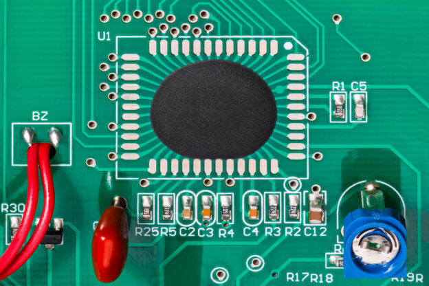
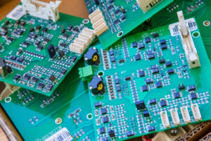
Lead-free assembly refers to production processes that eliminate the use of lead in solder and component finishes. Mandated by regulations such as RoHS compliance (Restriction of Hazardous Substances), this practice helps reduce toxic waste from electronic products at end-of-life. Customers and brands alike prioritize eco-friendly electronics, making lead-free assembly critical for market access and corporate responsibility.
One of the primary benefits of lead-free assembly is its environmental impact. Electronics that avoid lead reduce harmful contamination in landfills and recycling streams. Because electronics components often contain multiple materials, minimizing toxic substances simplifies recycling and supports circular manufacturing principles. BoardAssembly.com’s lead-free assembly options align with green manufacturing goals, making your products more appealing to eco-conscious consumers.
Lead-free processes also support workplace safety. Exposure to lead during assembly can pose health risks to workers. By transitioning to lead-free materials and soldering, manufacturers create a safer production environment. Proper training and equipment help ensure smooth integration of these processes without sacrificing quality or efficiency.
 Despite its advantages, lead-free assembly presents challenges. Lead-free solders typically have higher melting points, requiring adjustments in thermal profiles and equipment calibration. These differences demand skilled technicians and careful process validation to prevent defects such as tombstoning or poor wetting. Partnering with experienced manufacturers who specialize in PCB assembly and lead-free soldering helps mitigate these risks and achieve reliable outcomes.
For companies aiming to enter global markets, lead-free assembly is often non-negotiable. Many customers — from consumer electronics to industrial systems — require products that comply with international environmental standards. Choosing a manufacturing partner that understands compliance, documentation, and testing procedures ensures your products meet regulatory expectations.
In addition to environmental and compliance benefits, lead-free assembly can enhance brand reputation. Businesses that adopt sustainable practices differentiate themselves in crowded markets, appealing to partners and end users who value responsible manufacturing.
Ultimately, lead-free assembly reflects a broader commitment to ethical electronics production. Whether through component selection, process adjustments, or continuous quality monitoring, manufacturers play a key role in supporting sustainable technology ecosystems. For reliable lead-free assembly solutions that uphold quality and compliance, visit BoardAssembly.com and explore their comprehensive PCB assembly offerings.

 Another major advantage is improved supply chain management. Manufacturers with extensive industry experience can source components more efficiently and navigate global supply fluctuations. Contract electronics manufacturing partners monitor market conditions, secure parts early, and prevent costly production bottlenecks. This support is especially beneficial when demand spikes or tight lead times emerge.
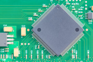
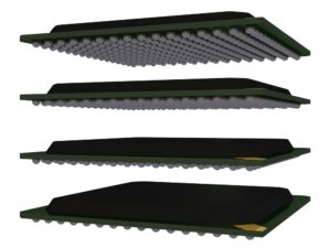 One of the primary advantages of BGA components is their enhanced electrical performance. By placing solder connections directly beneath the package, signals travel shorter distances with reduced parasitics, which boosts signal integrity. Improved thermal performance also helps distribute heat efficiently — critical for processors, FPGAs, and high-speed RF modules.
 Thru-hole assembly involves inserting electronic component leads into drilled holes on a PCB and soldering them in place. This process creates mechanically robust solder joints, superior to many surface mount options when it comes to withstanding vibration and thermal stress. Industries that demand long-life performance and high reliability often favor thru-hole components like connectors, large capacitors, transformers, and tall leaded components that simply cannot be mounted using SMT alone.
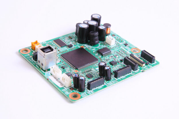
 Beyond mechanical assembly, Board Assembly also provides a full suite of value-added electronic services. These include firmware loading, software installation, device programming, calibration, and functional verification. Each unit undergoes thorough testing based on customer requirements—ranging from continuity checks and LED verification to complete system-level operational tests. This ensures the finished product is fully functional and deployment-ready upon delivery.


