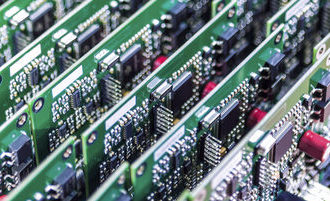
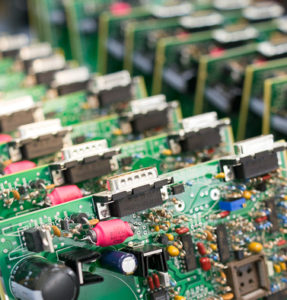
If you grew up taking apart radios, computers, or video game consoles just to see how they worked, you’ve likely studied a printed circuit board (PCB) up close. Among the intricate metallic traces and soldered components, you might have noticed small white letters, numbers, and symbols printed across the board’s surface. These markings aren’t random—they’re part of a critical layer called the PCB silkscreen.
Understanding the PCB Silkscreen Layer
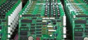 The PCB silkscreen is a printed layer that provides human-readable information on a circuit board. Typically created with special inks, the silkscreen identifies important features such as:
-
Component reference designators (like R1, C5, U2)
-
Test points
-
Warning symbols
-
Company logos
-
Part numbers and date codes
-
Polarity indicators for diodes, LEDs, and capacitors
Most PCB silkscreens are printed in white ink because it contrasts clearly with the traditional green solder mask. However, silkscreen inks can also be black, red, blue, or yellow, depending on the board’s color scheme or specific customer requests.
Why Is the Silkscreen Important?
The silkscreen acts as a visual guide for anyone who assembles, repairs, or tests the PCB. It tells workers how components should be placed and identifies key features to assist in troubleshooting and maintenance. Without a clear silkscreen, identifying the purpose or placement of components could quickly become confusing, leading to costly mistakes or longer assembly times.
Additionally, the silkscreen enhances safety by marking high-voltage areas or other hazards clearly.
How Silkscreens Are Applied
 Adding the silkscreen is typically the final step in PCB fabrication, done while the boards are still panelized. The ink used must be carefully chosen to withstand the chemicals and heat involved in soldering and assembly. Once printed, the board moves to the final finishing or routing phase.
There are several methods for applying a silkscreen:
-
Manual Screen Printing: Traditional, cost-effective for low-volume runs
-
Liquid Photo Imaging (LPI): Offers higher precision for dense, complex boards
-
Direct Legend Printing (DLP): Uses inkjet printers for extremely accurate and fast printing
Each method is selected based on the PCB’s design complexity, production volume, and budget.
Common Mistakes to Avoid in Silkscreen Design
Even experienced PCB designers can make mistakes when preparing the silkscreen layer. Some key things to watch out for:
-
Avoid printing over pads: Silkscreen ink can interfere with soldering and create defects.
-
Keep text legible: Fonts should be large enough to read easily, even after solder mask application.
-
Allow for registration tolerance: Slight shifts during manufacturing mean text and symbols should have enough spacing to stay clear and readable.
A well-designed silkscreen makes the PCB easier to work with and improves overall product quality.
 Trust ACME PCB for Quality PCB Manufacturing
At ACME PCB, we take pride in handling every detail of your PCB project—including the silkscreen layer. Our team ensures that every marking is clear, correct, and perfectly aligned, giving you boards that are not only functional but also easier to assemble, maintain, and troubleshoot.
Need a reliable PCB manufacturer that gets the details right? Contact ACME PCB today to get started!


