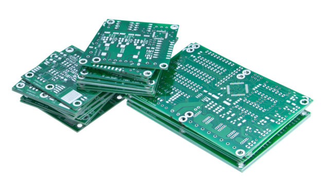
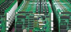
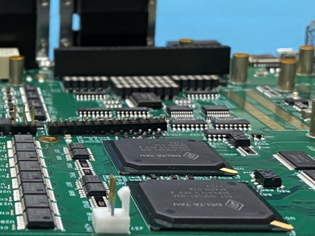
Printed circuit boards (PCBs) are the backbone of nearly every modern electronic device—from smartphones and automotive systems to medical equipment and industrial controls. As global electronics demand continues to rise in 2025 and beyond, the environmental impact of PCB manufacturing has become a central concern for manufacturers, engineers, and consumers alike. Today, sustainability is no longer a trend—it is a responsibility. Forward-thinking companies like Board Assembly are embracing eco-conscious manufacturing practices to reduce environmental impact while maintaining the highest quality standards.
Why Sustainability Matters More Than Ever
 PCB production is traditionally resource-intensive. It requires large amounts of raw materials, water, energy, and chemical processing. Without proactive sustainability efforts, these processes can contribute to carbon emissions, hazardous waste, and long-term environmental damage. At the same time, many OEMs and end users now demand greener supply chains. Regulatory pressure is increasing, and corporate responsibility expectations are higher than ever. Sustainable PCB manufacturing is now essential to long-term business success and global environmental stewardship.
Key Sustainable Practices in Modern PCB Manufacturing
Material Optimization
One of the most important steps toward sustainability starts with material selection. Today’s manufacturers increasingly rely on lead-free solders, halogen-free laminates, and RoHS-compliant components to reduce toxic exposure and improve recyclability. In addition, unused material from fabrication runs is now more frequently recovered and reused to minimize waste.
Energy Efficiency
Energy consumption remains one of the largest contributors to a PCB manufacturer’s carbon footprint. In 2025, many facilities are modernizing with high-efficiency SMT equipment, LED lighting, and optimized production workflows. Some manufacturers are also incorporating renewable energy sources such as solar power, significantly lowering overall emissions.
Advanced Chemical Management
Etching, plating, and surface finishing require chemicals that must be handled responsibly. Sustainable facilities invest in closed-loop chemical recycling systems, solvent recovery programs, and state-of-the-art wastewater treatment to prevent harmful discharge into the environment. These systems protect both the environment and worker safety.
Design for Sustainability
Engineers now play a direct role in environmental impact reduction through design for sustainability (DfS). Smaller PCB layouts, HDI designs, and optimized trace routing reduce material usage while increasing electrical performance. Multi-functional boards reduce the need for multiple assemblies, helping lower both manufacturing waste and energy consumption.
Recycling and End-of-Life Recovery
Electronic waste is one of the fastest-growing waste streams in the world. Sustainable PCB manufacturers now support recycling programs that recover valuable metals such as gold, copper, and silver from old circuit boards. This circular economy approach reduces demand for new mining while keeping harmful materials out of landfills.
The Business Advantages of Sustainable Manufacturing
Sustainability is not only good for the environment—it also makes strong business sense. Companies that adopt green manufacturing practices benefit from:
-
Lower long-term operational costs
-
Reduced regulatory risk
-
Stronger brand reputation
-
Increased appeal to environmentally conscious customers
-
Improved supply chain stability
In today’s competitive electronics market, sustainability is now a differentiator that directly influences purchasing decisions.
Partner with an Eco-Conscious PCB Manufacturer
 By selecting a manufacturer committed to sustainable production, businesses take an active role in protecting the environment without sacrificing performance or reliability. Board Assembly continues to emphasize environmentally responsible practices across its PCB fabrication and assembly services, delivering high-quality circuit boards that meet both engineering and environmental standards.
To learn more about sustainable PCB manufacturing, visit Board Assembly’s PCB Fabrication page and discover how innovation and environmental responsibility are shaping the future of electronics.
 The
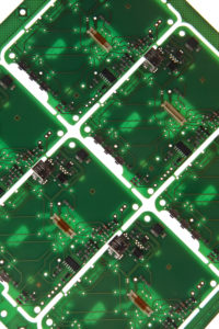
The  Adding the silkscreen is typically the final step in PCB fabrication, done while the boards are still panelized. The ink used must be carefully chosen to withstand the chemicals and heat involved in soldering and assembly. Once printed, the board moves to the final finishing or routing phase.
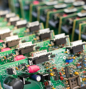 Trust ACME PCB for Quality PCB Manufacturing
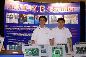
 Printed Circuit Boards (PCBs) are the backbone of modern electronics, found in everything from smartphones to medical devices.
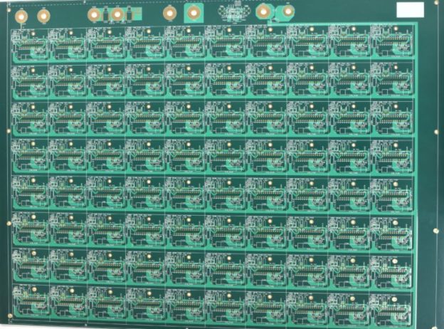
 ACME PCB Assembly is in Carson, California and provides the following services and more.


