Tag Archives: board assembly

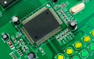
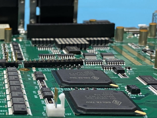
2 BGAs or More vertical installing.

The Rise of Package on Package (PoP) in PCB Assembly

In the ever-evolving landscape of electronics manufacturing, Package on Package (PoP) technology is transforming how circuit boards are designed and assembled. First gaining traction in the early 2000s, PoP is now considered one of the most innovative advances since the introduction of Ball Grid Array (BGA) components in the mid-1990s.

At its core, PoP is an integrated circuit packaging method that vertically stacks two or more BGA packages—typically combining a logic processor and memory component. This space-saving configuration allows for compact, high-performance assemblies ideal for smartphones, wearables, medical devices, and advanced industrial electronics.

The Advantages of PoP Technology

The primary benefit of PoP technology lies in its ability to reduce external pin count through package-level system integration. By stacking chips vertically, engineers can achieve a smaller footprint without sacrificing power or performance. This simplification not only optimizes PCB layout efficiency but also improves overall product reliability by minimizing interconnect lengths and signal interference.

Depending on the configuration, PoP packages can reach a total height as low as 1.4mm, making them perfect for compact devices where every millimeter counts. Additionally, PoP assemblies support independent testing of logic and memory layers, resulting in higher manufacturing yields and easier defect isolation during production.

ACME PCB Assembly: Leading the Way Since 2009

Since 2009, ACME PCB Assembly has been a leader in adopting and refining PoP technology. Utilizing advanced FUJI assembly lines and precise reflow soldering techniques, ACME delivers reliable PoP BGA assemblies for both prototype runs and medium-batch production.

From single-unit builds to production runs of up to 20,000 pieces, ACME’s skilled technicians ensure precise alignment, solder integrity, and quality control at every stage. This allows clients to seamlessly integrate high-density packaging into their next-generation designs—accelerating time to market while maintaining exceptional performance standards.

Whether you’re developing consumer electronics, industrial control systems, or medical devices, PoP technology offers a compact and efficient solution.

Embrace the Future of PCB Assembly

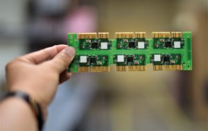
2 BGAs or More vertical installing.

ACME PCB Assembly is your trusted partner for Package on Package assembly, offering experience, precision, and scalability for your most advanced designs. Contact Board Assembly today at 310-715-1898 to learn how PoP can enhance your next project.

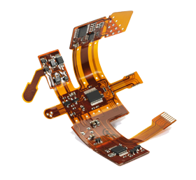
Flexible Circuit board

Trends in PCB Technology 2025: HDI, Flexible PCBs & Embedded Components

The world of printed circuit board (PCB) technology is evolving rapidly. As design demands grow denser, smarter, and more compact, three trends are defining the next generation of electronics: High-Density Interconnect (HDI), Flexible & Rigid-Flex PCBs, and Embedded Components. At Board Assembly, we’re keeping a close eye on these advances to ensure our clients stay ahead of the curve.

1. HDI: Packing More into Less

HDI technology enables PCBs with tighter trace spacing, smaller vias, buried and blind vias, and multiple layers of interconnects. These capabilities support miniaturization while maintaining signal integrity. In fact, Ultra-HDI is pushing the envelope even further, with features like microvias smaller than 2 mil and dense layer stacking becoming more commonplace in 2025.

For applications in high-speed communication, computing, and mobile devices, HDI is indispensable. It allows more functionality per square millimeter and reduces signal path length, which helps with high-frequency performance.

2. Flexible & Rigid-Flex PCBs: Form Meets Function

Rigid-flex and flexible PCBs bridge the gap between rigid boards and adaptable electronics. As IoT, wearables, and foldable electronics grow in importance, demand for flexible interconnects is rising sharply.

These flexible circuits allow boards to bend, fold, or conform to shapes, reducing connector count, saving space, and improving reliability. Designers are combining rigid and flex segments into single boards (rigid-flex) to gain mechanical stability where needed and flexibility where required.

In 2025, we’re seeing material innovations: thinner substrates, more durable flex films, and improved adhesion layers, all designed to survive repeated bending cycles and harsh environmental conditions.

3. Embedded Components: The Next Level of Integration

Embedded component technology involves placing passive and sometimes active devices (resistors, capacitors, ICs) within the layers or substrate of a PCB rather than on its surface. This approach reduces board surface complexity, shrinks form factors, and improves performance by shortening signal paths.

By embedding components, PCB designers can reduce external solder joints, minimize parasitic inductance, and better manage circuit density. This trend is especially relevant for compact, performance-sensitive sectors like aerospace, medical devices, and wearable electronics.


Printed Circuit Board FabricationWhy These Trends Matter for Your Projects
  • Smaller form factors: More capability in less space.

  • Better performance: Shorter interconnects, cleaner signal paths, less noise.

  • Reliability & durability: Fewer external interconnects, more mechanically robust designs.

  • Modern applications: These technologies enable cutting-edge devices in AI, 5G, IoT, and more.

At Board Assembly, we support HDI, flexible, rigid-flex, and embedded-component assemblies to meet the demands of tomorrow’s electronics. Whether you’re prototyping or producing in volume, we’re ready to partner with you.

Conformal Coating Spray

The Growing Importance of Conformal Coating in PCB Protection

Printed Circuit Boards (PCBs) are at the heart of modern electronics—but as devices become smaller, more powerful, and more widely used in harsh environments, protecting these sensitive components has become more critical than ever. That’s where conformal coating in PCB protection steps in as a game-changer.

Whether it’s a consumer product exposed to daily wear or a military-grade device deployed in extreme climates, PCBs need an added layer of protection. Conformal coating provides exactly that: a thin, durable film that safeguards electronics from moisture, dust, chemicals, and temperature extremes without compromising performance or size.

Solder Mask on Printed Circuit BoardsWhat Is Conformal Coating?

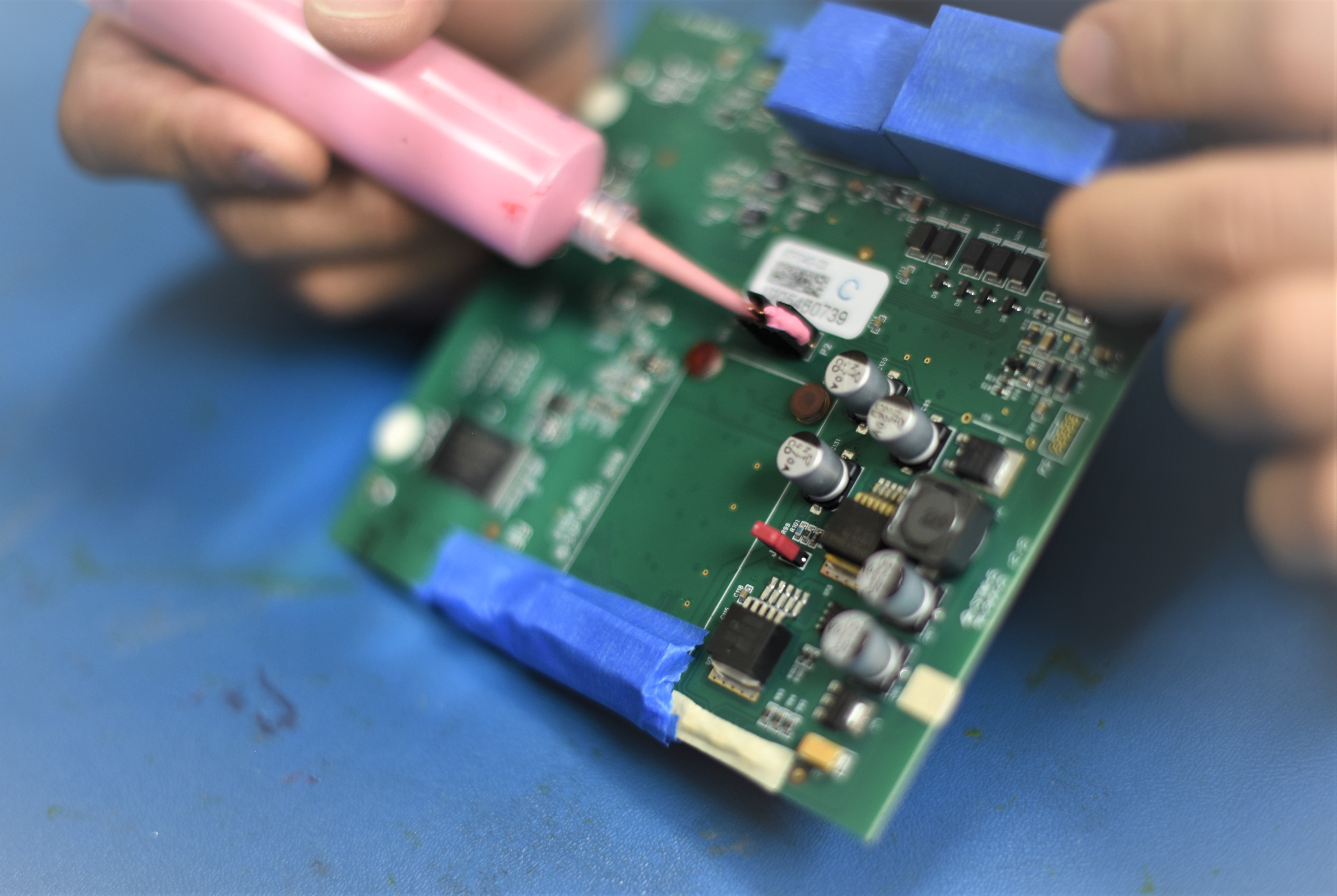
conformal coating maskingconformal coating maskingConformal coating is a protective chemical layer applied to the surface of a PCB to create a barrier against environmental contaminants. It’s “conformal” because it conforms to the shape of the board and its components, coating even hard-to-reach areas without needing bulky enclosures.

At Board Assembly, we apply conformal coatings using precise, industry-approved techniques that ensure full coverage without interfering with the function or accessibility of electronic parts.

Why Is Conformal Coating Becoming More Important?

As electronics continue to expand into sectors like automotive, aerospace, defense, and IoT devices, the environments these PCBs operate in are becoming more unpredictable and challenging.

Here are a few key reasons conformal coating is gaining traction:

  • Moisture & Corrosion Resistance: In humid or marine environments, moisture can cause corrosion, short-circuits, and long-term failure. Conformal coatings seal off the PCB surface, keeping moisture at bay.

  • Chemical Protection: In industrial settings, exposure to cleaning agents, fuels, or harsh chemicals is common. A conformal coating acts as a shield, preventing chemical damage.

  • Dust & Debris Protection: For electronics in outdoor or manufacturing environments, dust accumulation can hinder performance. Coatings protect against particulate buildup.

  • Extended Product Life: By protecting the PCB from environmental damage, conformal coatings significantly increase product reliability and longevity—essential for industries where equipment failure is not an option.

Applications Across Industries

From automotive control units to aerospace avionics, and from wearable medical devices to outdoor smart home systems, conformal coating in PCB protection is now a standard best practice in many industries. As miniaturization and high-performance demands increase, protective coatings are no longer optional—they’re essential.

Why Work With Board Assembly?

At Board Assembly, we offer advanced PCB assembly solutions that include precision-applied conformal coatings to ensure your product performs reliably in any environment. Whether you need protection from moisture, vibration, chemicals, or dust, our team ensures your PCB is ready for real-world conditions.


Want to learn more about how conformal coating can improve your product’s performance and durability? Contact us today to discuss your PCB protection needs.

pcb-fabrication-and-assembly-in-usa

How to Choose the Right PCB Material for Your Application

When it comes to electronic products, the materials you choose for your printed circuit board (PCB) can make all the difference in performance, reliability, and even cost. Selecting the right PCB material isn’t just about picking what’s readily available; it’s about matching the material’s properties to your specific application. At Board Assembly, we understand the importance of PCB material selection and are here to help you navigate the options.

Why PCB Material Matters

Your PCB is the backbone of your electronic device. It carries electrical signals, manages heat, and supports all your components. The wrong material choice can lead to issues like signal loss, overheating, or even mechanical failure. That’s why understanding your project’s requirements is key to making the right choice.

Factors to Consider

  1. Thermal Performance:
    If your application generates a lot of heat—like in power electronics or LED lighting—you’ll need a PCB material with good thermal conductivity. Materials like aluminum-based PCBs or high-Tg FR-4 are excellent choices.

  2. Electrical Performance:
    For high-frequency or RF applications, you’ll need a material with low dielectric loss. PTFE-based materials are often recommended for their superior electrical properties.

  3. Mechanical Strength:
    Will your PCB be exposed to vibrations, shock, or mechanical stress? If so, choose materials with higher mechanical strength to avoid cracks and failures.

  4. Cost:
    Budget matters too. While advanced materials like Rogers or ceramic substrates offer excellent performance, they can be pricey. For many applications, standard FR-4 remains a reliable and cost-effective option.

  5. Environmental Conditions:
    Consider the environment your PCB will operate in. Will it face moisture, chemicals, or extreme temperatures? Some materials offer better resistance to harsh conditions.

Trust Board Assembly with Your PCB Needs

At Board Assembly, we guide our customers through every step of the PCB material selection process. Our team helps you find the perfect balance between performance and budget, ensuring your project is a success.

📞 Contact us today to learn more about our services and how we can help you choose the best PCB material for your application.

Printed Circuit Boards

What is a PCB Silkscreen on Printed Circuit Boards?

If you grew up taking apart radios, computers, or video game consoles just to see how they worked, you’ve likely studied a printed circuit board (PCB) up close. Among the intricate metallic traces and soldered components, you might have noticed small white letters, numbers, and symbols printed across the board’s surface. These markings aren’t random—they’re part of a critical layer called the PCB silkscreen.

Understanding the PCB Silkscreen Layer

The PCB silkscreen is a printed layer that provides human-readable information on a circuit board. Typically created with special inks, the silkscreen identifies important features such as:

  • Component reference designators (like R1, C5, U2)

  • Test points

  • Warning symbols

  • Company logos

  • Part numbers and date codes

  • Polarity indicators for diodes, LEDs, and capacitors

Most PCB silkscreens are printed in white ink because it contrasts clearly with the traditional green solder mask. However, silkscreen inks can also be black, red, blue, or yellow, depending on the board’s color scheme or specific customer requests.

Why Is the Silkscreen Important?

The silkscreen acts as a visual guide for anyone who assembles, repairs, or tests the PCB. It tells workers how components should be placed and identifies key features to assist in troubleshooting and maintenance. Without a clear silkscreen, identifying the purpose or placement of components could quickly become confusing, leading to costly mistakes or longer assembly times.

Additionally, the silkscreen enhances safety by marking high-voltage areas or other hazards clearly.

How Silkscreens Are Applied

Printed Circuit Board FabricationAdding the silkscreen is typically the final step in PCB fabrication, done while the boards are still panelized. The ink used must be carefully chosen to withstand the chemicals and heat involved in soldering and assembly. Once printed, the board moves to the final finishing or routing phase.

There are several methods for applying a silkscreen:

  • Manual Screen Printing: Traditional, cost-effective for low-volume runs

  • Liquid Photo Imaging (LPI): Offers higher precision for dense, complex boards

  • Direct Legend Printing (DLP): Uses inkjet printers for extremely accurate and fast printing

Each method is selected based on the PCB’s design complexity, production volume, and budget.

Common Mistakes to Avoid in Silkscreen Design

Even experienced PCB designers can make mistakes when preparing the silkscreen layer. Some key things to watch out for:

  • Avoid printing over pads: Silkscreen ink can interfere with soldering and create defects.

  • Keep text legible: Fonts should be large enough to read easily, even after solder mask application.

  • Allow for registration tolerance: Slight shifts during manufacturing mean text and symbols should have enough spacing to stay clear and readable.

A well-designed silkscreen makes the PCB easier to work with and improves overall product quality.

Turnkey Yun IndustrialTrust ACME PCB for Quality PCB Manufacturing

At ACME PCB, we take pride in handling every detail of your PCB project—including the silkscreen layer. Our team ensures that every marking is clear, correct, and perfectly aligned, giving you boards that are not only functional but also easier to assemble, maintain, and troubleshoot.


Need a reliable PCB manufacturer that gets the details right? Contact ACME PCB today to get started!