 With everyone’s increasing concerns on the over usage of hazardous materials in the electronic and electrical products and their environmental impact, there have been several stricter regulations being imposed by the leading governmental organizations across the world. The RoHS compliance is one of those important regulations that is currently being imposed on the utilization of hazardous materials in the electronics and electrical products. Are you interested in knowing how this compliance works or what the benefits are?
Being Able to Understand the Materials that are Restricted Under RoHS Compliance
The RoHS compliance has restricted the use of six materials in the PCBs and electronic items. They include Mercury (Hg), Lead (Pb), Cadmium (Cd), Hexavalent Chromium (CrVI), polybrominated diphenyl ethers (PBDE), Polybrominated biphenyls (PBB), and phthalates such as BBP, DEHP, BBP, and DIBP.
The compliance also specifies the maximum levels of these restricted materials in the PCBs and other electronics items.
- Mercury (Hg): < 100 ppm
- Lead (Pb): < 1000 ppm
- Cadmium (Cd): < 100 ppm
- Polybrominated Biphenyls (PBB): < 1000 ppm
- Hexavalent Chromium: (Cr VI) < 1000 ppm
- Polybrominated Diphenyl Ethers (PBDE): < 1000 ppm
- Bis(2-Ethylhexyl) phthalate (DEHP): < 1000 ppm
- Dibutyl phthalate (DBP): < 1000 ppm
- Diisobutyl phthalate (DIBP): < 1000 ppm
- Benzyl butyl phthalate (BBP): < 1000 ppm
The Many Features of RoHS-Compliant Assembly Services
Many PCB assembly services are utilizing processes and technologies that help them manufacture RoHS-compliant PCB assemblies. The following are a few features that help distinguish these services from others.
- Lead-free Surface Finishes:Many manufacturers are nowadays using lead-free surface finishes such as lead-free HASL, ENIG, Electroplated Nickel and Soft (Bondable), Hard Gold Immersion Tin (White Tin), and Organic Solderability Preservatives (OSP).
- RoHS Compliant Substrate Materials:The choice of RoHS material depends on the requirement of the application. There are materials such as Isola IS410, and Polyclad 370HR that assure standard electrical performance; however, materials such as Isola FR415 and Polyclad Getek assure high electrical performance at low loss.
- Primary and Secondary Services:It has been observed that many RoHS PCB assembly service providers specialized in primary and secondary services such as lead trimming, lead-free wave soldering, and many more.
Some Benefits of Using RoHS-Compliant PCBs
The benefits that are offered by lead-free and RoHS-compliant PCBs are various. The following are a few of them:
- Helps Reduce Metal Poisoning:As the technology landscape is fast evolving, many customers are discarding their obsolete electronic equipment in landfills. Equipped with various hazardous materials, this equipment helped lead to severe poisoning. Although recycling is being performed, still the equipment may have hazardous substances in them. The RoHS directive has forced OEMs reduce their dependence on hazardous substances. This has helped reduce the impact of these materials on the environment, and people working with them.
- Improved Product Safety:With RoHS compliance being adopted by many prominent electronics manufacturers in EU and the US, now users can be assured that the product they are using is lead and mercury free. As a result, the sales and popularity of the products from these manufacturers has tremendously increased.
- Improved Thermal Properties:It is proven that lead-free PCBs have excellent thermal properties than their leaded counterparts. They can easily withstand temperatures between -45°C to 145°C. Nowadays, PCB manufacturers are using specialized halogen-free laminates that have further helped improve their thermal stability up to 300 °C.
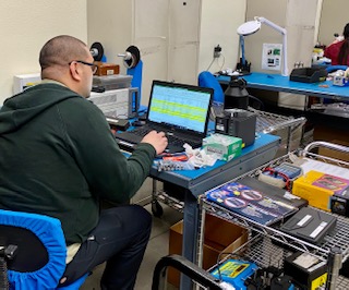
The benefits of RoHS-compliant PCBs symbolize a green future. It is important that you find a trusted RoHS-compliant assembly services provider such as Yun Industrial and ACME PCB Assembly. Our company follows processes that are audited regularly and certified as chemical free.
Call today to find out more about our RoHS-compliant assembly services.
 Flexible PCB Assembly for Every Project Size
 Thermal Performance:
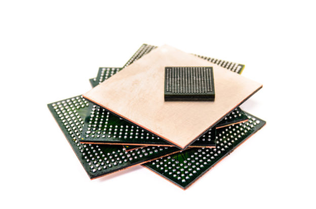
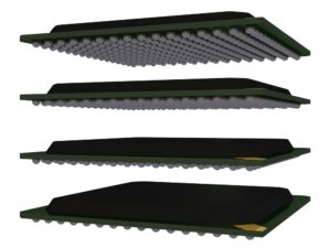 BGA assembly is a type of SMT process, which is used for
 The
The 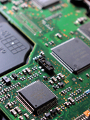 Adding the silkscreen is typically the final step in PCB fabrication, done while the boards are still panelized. The ink used must be carefully chosen to withstand the chemicals and heat involved in soldering and assembly. Once printed, the board moves to the final finishing or routing phase.
 Trust ACME PCB for Quality PCB Manufacturing


