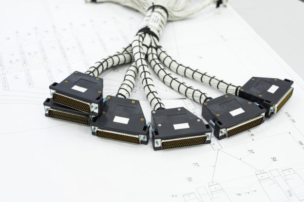
Cable Harnesses (Wire harness, cable assembly, wiring assembly) is an assembly of electrical cables or wires which transmit signals or electrical power. Cable harnesses are different from wire harnesses and it is important to understand the difference. A wire is a single conductor, while cables are two or more wires that are insulated being wrapped in a larger jacket. These two technologies demand their own set of unique tools, fixtures, and machinery to help reduce production costs. Knowing exactly what type of product being used is crucial to perfectly create your designs.
· Wire harnesses generally do not need much to work with and is generally an inexpensive and cost-efficient way for many people to solve their electrical needs. With a single machine, one can increase their production capabilities because of the relative simplicity of wires in general.
· Cable harnesses are more complex in nature and may require different machinery and tools to be consistent with production. Creating slits and windows in cables demand specialized equipment to handle the various conductors within the insulation
Both technologies are held to the standards like IPC WHMA-A-620 and should be evaluated by their designated class level.
Located in Carson, California, ACME PCB Assembly utilizes top of the line technology from Schleuniger to perfectly cut, strip, and process any wire or cable you need. After 25 plus years in the business, ACME PCB Assembly has the experience to be your contract manufacturer for cable & wire harness projects. As an IPC-A-610 certified assembler with a certified trainer in house, you can be rest assured the cables and wires that come out of ACME will exceed the standards.
You can rely on ACME PCB Assembly for timely, cost-effective service.
Contact Us for more information.
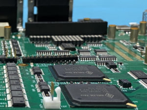 Find Your SMT and Through-Hole Vendor
 The
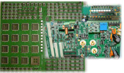
The  Adding the silkscreen is typically the final step in PCB fabrication, done while the boards are still panelized. The ink used must be carefully chosen to withstand the chemicals and heat involved in soldering and assembly. Once printed, the board moves to the final finishing or routing phase.
 Trust ACME PCB for Quality PCB Manufacturing
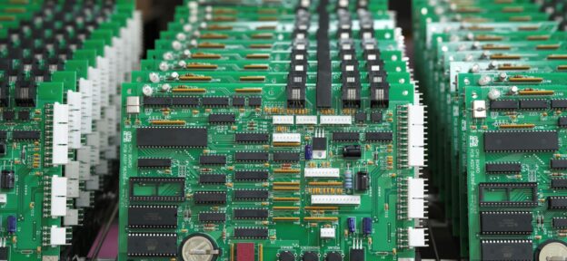
 1. Understand Your Application Requirements
 Choosing the right