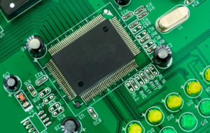
When electronic assemblies are exposed to moisture, chemicals, vibration, dust, or extreme temperature fluctuations, ordinary protection simply isn’t enough. Sensitive components require a higher level of defense to maintain long-term reliability. Potting and encapsulation services provide some of the most robust environmental protection available by fully surrounding electronic assemblies with epoxy, silicone, or urethane compounds. At Board Assembly, we specialize in delivering professional, application-specific potting and encapsulation solutions designed to improve performance and extend the lifespan of your products.
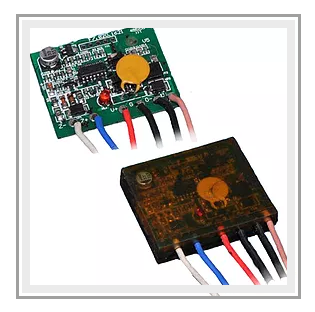
Potting involves filling an electronic assembly’s enclosure with a liquid insulating compound. Once cured, the compound becomes a rigid or semi-flexible protective shield that isolates components from environmental damage. Encapsulation, while similar, often uses removable molds or specialized housings designed to protect the electronics without requiring a permanent enclosure. Both processes are widely used in industries that demand rugged, field-ready electronics capable of withstanding harsh conditions.
Our potting and encapsulation services begin with a detailed evaluation of your product’s operating environment. Choosing the right material is essential. Epoxy provides high hardness and outstanding chemical resistance, making it ideal for industrial machinery or chemical exposure environments. Silicone is well suited for applications requiring flexibility, high thermal resistance, or vibration absorption. Urethane offers a balanced combination of shock absorption and durability, commonly used in automotive and consumer electronics.
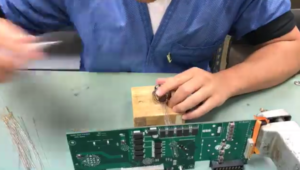
Before the potting process begins, each PCB is prepared through a thorough cleaning procedure to remove dust, flux residue, and contaminants that could affect adhesion. Sensitive areas such as connectors, LEDs, switches, and test points are masked to prevent compound coverage. Once prepared, the potting compound is precisely mixed, degassed to eliminate trapped air, and dispensed carefully to ensure even distribution. This helps prevent voids, which can compromise insulation or structural stability.
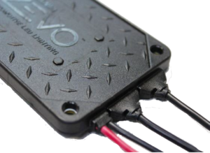
Potting and encapsulation provide a wide range of advantages. By sealing the assembly, the compound prevents moisture intrusion, corrosion, oxidation, and electrical arcing. Mechanical stability is improved, making the PCB more resistant to vibration, shock, and handling stress. The process also offers enhanced electrical insulation, allowing high-voltage components to operate safely. Additionally, potting provides tamper resistance, protecting proprietary circuits and preventing unauthorized access.
 Industries that rely heavily on these services include automotive electronics, outdoor communication systems, aerospace and defense equipment, marine technology, renewable energy systems, and rugged industrial controls. Any application exposed to environmental hazards can benefit from the long-term reliability provided by professional potting and encapsulation.
After curing, every assembly undergoes a meticulous inspection and functional test to ensure that the protective compound has not affected performance or accessibility. Documentation, traceability, serial labeling, and quality reports are included for customers in regulated industries.
For manufacturers seeking durable, reliable, and long-lasting electronics, potting and encapsulation are essential steps in the production process. At Board Assembly, our expertise and precision processes ensure superior results for every project.
Learn more about our potting and encapsulation services:
https://boardassembly.com/potting-and-encapsulating-services/
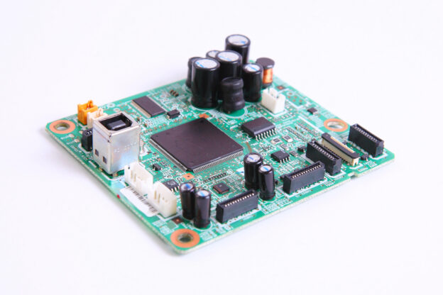
 Beyond mechanical assembly, Board Assembly also provides a full suite of value-added electronic services. These include firmware loading, software installation, device programming, calibration, and functional verification. Each unit undergoes thorough testing based on customer requirements—ranging from continuity checks and LED verification to complete system-level operational tests. This ensures the finished product is fully functional and deployment-ready upon delivery.
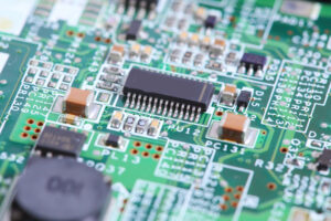 Our process begins with thorough PCB cleaning, ensuring no contaminants interfere with adhesion. Depending on the project, we apply coatings using automated selective coating systems, brushing, spraying, or dipping. Complex assemblies with connectors, switches, or areas requiring masking are handled precisely, preventing material from covering critical contact points.
 Once the assembly begins, solder paste is applied using tightly controlled stencil printing methods. This ensures proper solder volume, which is critical for component adhesion and long-term performance. Our automated reflow ovens use multi-zone temperature profiling to ensure consistent solder joints across every PCB. Whether your project requires leaded or RoHS-compliant lead-free soldering, Board Assembly adheres to strict temperature controls that guarantee reliability.
 PCB production is traditionally resource-intensive. It requires large amounts of raw materials, water, energy, and chemical processing. Without proactive sustainability efforts, these processes can contribute to carbon emissions, hazardous waste, and long-term environmental damage. At the same time, many OEMs and end users now demand greener supply chains. Regulatory pressure is increasing, and corporate responsibility expectations are higher than ever. Sustainable PCB manufacturing is now essential to long-term business success and global environmental stewardship.
 By selecting a manufacturer committed to sustainable production, businesses take an active role in protecting the environment without sacrificing performance or reliability.


