Author Archives: Erin

PCB Fabrication near me

Finding Electronic Turn-Key Assembly Manufacturing Services in the USA

Most entrepreneurs and manufacturers sometimes think the old ways of manufacturing electronics and printed circuit board manufacturing can be very intimidating because it is a slow process that can be prone to errors, and also expensive, which makes people hesitant to use it. Electronic turn-key assembly manufacturing wasn’t designed for small batch runs and prototypes, but to help support enormous orders with a long lead time. Luckily, the services of Turnkey Printed Circuit Board ( PCB) assembly are coming in today to meet the needs of hardware designers.

What is Turnkey Printed Circuit Board Assembly?

It is a new method to an electronic assembly that is influenced by onshore PCB manufacturing and cloud-based software to generate emerging printed circuit boards stress-free and fast for entrepreneurs, manufacturers, engineers, and small enterprises. 

Turnkey PCB assembly is taken beyond just printed circuit boards by some services and offers the service that is essential to come out with your completed products. Your product will be assembled as needed and the record of your part will be retained.

pcb-fabrication-and-assembly-in-california

People who can use Turnkey PCB Assembly

Anyone with a design can quickly at an affordable price bring out their new ideas because this new method of printed circuit board manufacturing eliminates all the limitations of quantity and cost in the legacy system. For all the startups and small enterprises that want to bring their products to market without risk and cost of big inventories, Turnkey PCB assembly is just the ideal approach to use. Also, it can be beneficial for kick-starter manufacturers who might not know whether they’ll require just hundreds or few boards. The flexibility and speed of instant PCB construction are also enjoyed by producers and hobbyists. Engineers in large enterprises also see it to be faster, easier and, more fascinating than traditional approaches.

At ACME PCB Assembly, we set high standards for the efficiency, quality and speed of our performance. Our turn-key supplies chain management solution, worldwide network of resources.

BGA-boards

The Benefits of Package-on-Package Assembly

Package-on-Package (PoP) is a type of IC packaging method that combines ball grid array (BGA) packages. In this method, two or more packages are vertically installed (i.e. stacked) with an interface that can direct signals between them.

BGA-boardsThere are two popular configurations for PoP assemblies:

  • Pure Memory Stacking: multiple memory packages are stacked on each other
  • Mixed Logic-Memory Stacking: a memory package is stacked on top of a CPU package

The packages are stacked on each other and attach to each other during reflow soldering.

There are several advantages PoP assembly has over tradition packaging methods:

  • Package-on-Package assembly more efficiently uses space, as packages are stacked vertically, increasing the effective space on the motherboard. The reduced space requirements for PCB assemblies caused by package-on-package assembly allowed smartphones and other compact electronic devices to achieve higher levels of performance without increasing in size.
  • Package-on-Package assembly also shortens the track length between components, causing better electrical performance as the shorter length will reduce noise and cross talk, and promote faster signal response.
  • Memory packages stacked in this fashion can be tested separately from the CPU package.
  • As long as the memory package fits on the CPU package, any memory package can be used, increasing flexibility in design.

Package-on-Package assembly is a delicate process and you should rely on an experienced and reliable PCB assembler such as IPC A-610 certified company like ACME PCB Assembly to build your products.

Whether you need Printed Circuit Board (PCB) assembly, consignment assembly or turnkey material-procurement assembly, we have what is necessary to manage your entire project efficiently. With over 26 years of experience in Electronics Manufacturing Services (EMS) we learned that reasonable assembly cost, high-quality service, on-time delivery and good communications are the keys that keep our customers happy and is how we made our business successful.

To find out more, call us at 310-715-1898

Printed circuit board production

uBGA Assembly on Double Sided Flex Circuit Board

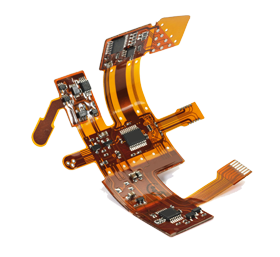
There are many benefits of uBGA Assembly on Double Sided Flex Circuit Board offered by the Acme PCB Assembly, beginning with the fact it can considerably improve the physical characteristics of a design by reducing both weight and size. The cost and performance advantages of using uBGA Assembly on Double Sided Flex Circuit Boards are also quality points that engineers and designers keep in mind, since this technology is used in many types of industries.

ACCURATE, EFFICIENT uBGA ASSEMBLY ON DOUBLE SIDED FLEX CIRCUIT BOARD

A correctly constructed uBGA assembly on double sided flexible circuit board is at the heart of many successful product production operations. Flexible Circuit board assembly and design is a complex, specialized process, which is why many companies choose to outsource this task to a PCB assembly provider that has the capability to get the job done properly and promptly. If you need high-grade uBGA Assembly on flexible printed circuit board that results in a high-performance solution to your manufacturing requirements, Acme PCB Assembly can help.

If you need help with Ball Grid Array (BGA/uBGA) assembly on a double sided flex circuit boards contact us today and we can give you a quote for your next project.

DOUBLE SIDED FLEX CIRCUIT BOARD PERFORMANCE VS RIGID PCB

  • Superior heat dissipation.
  • Dynamic Flexing.
  • Lower inductance (vs traditional wiring systems).
  • Superior package density.

PRINTED CIRCUIT BOARD ASSEMBLY COMPANY TO MEET YOUR DEADLINES

ACME PCB Assembly uses the most advanced equipment for the development and manufacturing of high performance uBGA Assembly on Double Sided Flex Circuit Board . ACME PCB Assembly has equipment and processes which allow us to offer our customers a flexible, cost-effective, and quality-focused assembly. ACME understands the challenges companies face for their projects. ACME Flexible PCB Assembly is able to accommodate large orders while getting the work done within the the time expected.

To find out more, call us at 310-715-1898

BGA inspection

Understanding BGA Assembly Technology

A Ball Grid Array or (BGA) is a SMT (Surface Mount Technology) package that is most commonly used for Integrated Circuits (ICs) with a large number of pins. Ball grid array packaging is a method for reducing package size and integrating a greater number of functions on a single chip module.

With it being a high-density and low-cost packaging option, this technology helps create the best range of circuit boards with precision component placement and soldering excellence.  BGA (Ball Grid Array) also replaces solder balls on the component underside for SMT mounting.  ACME PCB assembly has capabilities that include (ball grid array) BGA assembly and rework up to 65mm squared up to 36-layer printed circuit board.

BGA technology, which uses an array of solder balls for electrical interconnection, offers up several advantages over pin-grid array (PGA).  A couple important advantages of this surface-mount package is:

  • Ball Grid Array enables assemble boards with reduced thickness. This is beneficial when it comes to making sleek electronic products like smart phone, and tablets.
  • They seldom require maintenance and repair.
  • The packaging is more stable because there are no pins that can be bent and broken.
  • Excellent improvement in both thermal and electrical performance, which efficiently uses the space of the circuit board.
  • BGA packaging is compatible with high-efficiency system products.

ACME Printed Circuit Board Assembly started it’s (Ball Grid Array) BGA assembly service in 1994.  With so many years of experience in BGA assembly with X Ray inspection machine, and having the right assembly procedure in place, we are confident in saying that we can build a high quality, good yield rate BGA assembly board.

ACME Printed Circuit Board Assembly is an EMS located in Southern California near Los Angeles airport, it especially for Small to Medium run PCB assembly. Our workmanship meets IPC 610 standard. ISO 9001:2015 certified manufacturer for Electronics Contract manufacturing since Year 2000.

ACME PCB assembly also does BGA prototype assembly for our customers. We are able to create a BGA prototype assembly with or without stencil to help save our customer’s prototyping cost.

Please contact us 310-715-1898, or email us if you have any question.


Printed Circuit Board Fabrication

What is a PCB Silkscreen on Printed Circuit Boards?

What is a PCB Silkscreen on Printed Circuit Boards?

Were you one of those kids who loved to take apart every electronic thing in your house? If so, you’ve probably pulled out your fair share of green printed circuit boards. It’s cool to hold them and to run your fingers over all their little metallic bumps. When you brought them close to your eye, you could even see little white designs, numbers, and letters drawn on them. What is this mysterious language? It’s called the PCB silkscreen.

The PCB Silkscreen

Silkscreen is the white and human readable letters, normally used to identify components, test points, PCB and PCBA part numbers, warning symbols, company logos, date codes and manufacturer marks.  Silk-screening requires specially formulated inks. The standard color is white, but you can also select red, blue, black, yellow, etc.  Most silkscreens are written in white ink, because it is easy to see against the green solder-mask, but silkscreens can actually be any color. If you take apart enough electronics, you are bound to find PCBs with gray, red, and even blue silkscreens.

Adding the silkscreen layer onto a printed circuit board is the final step in the fabrication process. These shapes, numbers, and letters really aren’t some new language. They act as basically an instruction manual, telling workers how to assemble the board as part of the larger device. They can also communicate the function of each of the pins.  Screen-printing is done when the boards are still penalized prior to the application of the final finish or routing/v-scoring.

PCB layout designers sometimes forget to double-check their silk screen layers before sending designs to PCB fabrication. Designers should avoid putting ident over component pads, they should avoid using excessively tiny text and should allow for registration tolerances.

Looking for a new PCB manufacturer? Contact ACME PCB today.