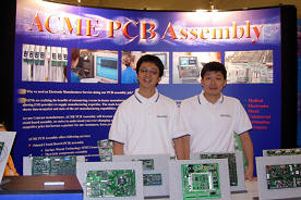
Providing Electronics Manufacturing Services (EMS) Since 1993
The electronic manufacturing services (EMS) industry took off after the late 1970’s. Before this, most electronics manufacturing that was done in large quantity production runs was handled by in-house assembly only.
Now, the electronic manufacturing services (EMS) provider offers more flexibility and easier resources to deal with issues for smaller companies who doing limited runs. An electronic manufacturing services (EMS) provider is able to specialize in large manufacturing, raw materials procurement, and resources.
 Since the early 1990’s, the development of Surface Mount Technology (SMT) on PCB has allowed for the rapid assembly of electronics, many electronic components switched to Surface Mount Technology (SMT) from Through hole components. SMT components are making more and more small footage, more and more fine pitch, the equipment for SMT components are requiring more and more accuracy. For small businesses, it is a good idea to outsource your EMS needs.
Outsourcing all your manufacturing needs to a Electronic manufacturing services (EMS) provider helps you to save money, it also helps you to control your overhead cost, which in turn reduces your companies overhead cost. As a result, Electronic manufacturing services (EMS) provider gives you the opportunity to produce your products at a lower cost.
ACME PCB Assembly in Carson, California has been an Electronic manufacturing services (EMS) provider since 1993. OEMs are realizing the benefits of outsourcing versus in-house manufacturing. Outsourcing to Electronic manufacturing services (EMS) provider enables OEMs to concentrate on their core competencies by allowing Electronic manufacturing services (EMS) providers to supply manufacturing expertise. The main benefits of outsourcing include a reduction in costs and investment, additional capacity, shorter time-to-market and state-of-the-art manufacturing capabilities.
As your Contract manufacturer, ACME circuit board assembly will become a business partner who has a vested interest in your success. By outsourcing to ACME circuit board assembly, ACME PCB Assembly strive to understand your ever-changing needs in your specific competitive markets. Our objective is to provide not only quality products with a competitive price but become a partner for our customer, from product design to the distribution process.
 What Is a Contract Electronic Manufacturing Service Provider?
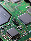 Industries That Benefit from PCB Assembly Services
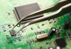 Partner with a Trusted PCB Assembly Provider
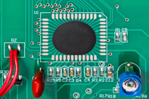
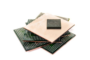 BGA (Ball Grid Array) is a surface-mount packaging technology that enhances electrical and thermal performance in PCBs. Unlike traditional dual in-line or quad flat packages, BGA uses an array of solder balls beneath the component rather than protruding pins. These solder balls establish electrical connections to the PCB, offering better heat dissipation, signal integrity, and mechanical stability.
 While BGA Assembly offers numerous benefits, ensuring flawless soldering and defect-free connections is crucial. Advanced techniques like X-ray inspection and reflow soldering help detect hidden defects and guarantee the highest level of precision.
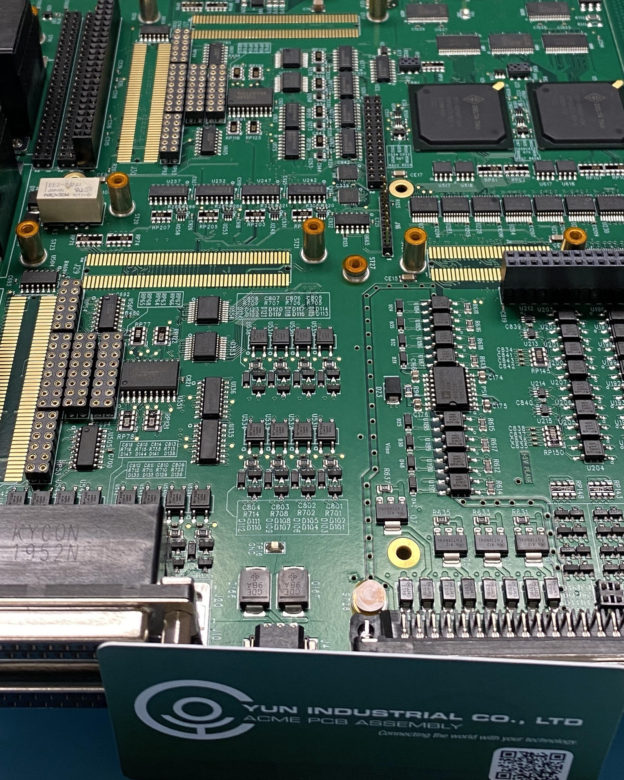
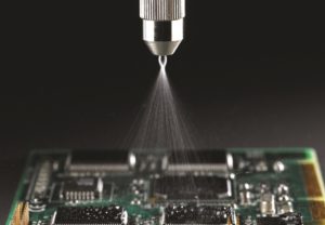
 ACME PCB Assembly happens to offer three different kinds of conformal coating for our valuable customers. The acrylic conformal coating is a low viscosity coating that is cured through drying and isn’t too resistant to chemicals but hardens quickly. The Urethane conformal coating is also a low viscosity coating, however, is cured through crosslinking with strong resistances to chemicals. Silicone conformal coating is a very viscous coating that is applied through swirl technology with high chemical resistances.


