In today’s fast-paced electronics industry, businesses rely on contract electronic manufacturing service providers to streamline their production processes. Whether you need prototypes or full-scale production, partnering with a reliable manufacturer ensures high-quality PCB assembly and efficient turnaround times.
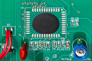 What Is a Contract Electronic Manufacturing Service Provider?
A contract electronic manufacturing service (CEMS) provider specializes in producing electronic components, circuit boards, and complete assemblies for various industries. These manufacturers handle everything from PCB fabrication and PCB assembly services to quality testing and final product integration.
Why Partner with a Contract Manufacturer for PCB Assembly?
Choosing a reputable PCB assembly provider brings several advantages, including:
1. Expertise and Precision
Professional manufacturers use cutting-edge technology and industry best practices to ensure precise and high-quality PCB assembly services. Their expertise in surface-mount technology (SMT), through-hole technology (THT), and mixed-technology assembly results in reliable products.
2. Cost Savings and Efficiency
In-house PCB production requires significant investment in equipment, materials, and skilled labor. Outsourcing to an experienced contract electronic manufacturing service reduces overhead costs while improving efficiency.
3. Scalability for Production Demands
Whether you need small-batch prototyping or large-scale production, contract manufacturers adjust their capacity to meet your needs. This flexibility allows companies to scale their production based on demand.
4. Quality Assurance and Compliance
A trusted PCB assembly services provider follows strict industry standards such as ISO 9001, IPC-A-610, and RoHS compliance, ensuring that every PCB meets high-quality benchmarks.
5. Faster Time-to-Market
With streamlined manufacturing processes and supply chain management, contract manufacturers help companies bring products to market quickly without compromising quality.
 Industries That Benefit from PCB Assembly Services
Various industries depend on PCB assembly for their electronic components, including:
- Aerospace & Defense – High-reliability PCBs for mission-critical systems
- Medical Devices – Precision electronics for patient monitoring and diagnostics
- Automotive – Advanced circuit boards for electric vehicles and infotainment systems
- Consumer Electronics – Smartphones, wearables, and smart home devices
- Industrial Automation – Control systems and IoT devices for smart manufacturing
Choosing the Right PCB Assembly Partner
When selecting a contract electronic manufacturing service provider, consider the following factors:
- Experience & Capabilities – Ensure they offer comprehensive PCB fabrication and assembly services.
- Certifications & Compliance – Look for ISO, IPC, and RoHS certifications.
- Prototyping & Mass Production – Check if they can handle both small and large volumes.
- Customization & Engineering Support – Choose a provider that offers design and engineering assistance.
- Customer Support & Communication – A responsive team ensures smooth project execution.
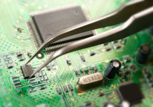 Partner with a Trusted PCB Assembly Provider
Finding the right PCB assembly services provider can make all the difference in the success of your electronic products. If you’re looking for high-quality PCB fabrication and assembly solutions, BoardAssembly.com offers state-of-the-art manufacturing services tailored to your needs.
Explore their advanced capabilities and experience seamless PCB assembly services for your next project.
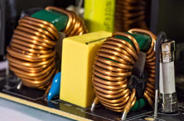
 ACME PCB Assembly is in Carson, California and provides the following services and more.


