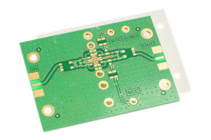
 Printed Circuit Boards (PCBs) are the backbone of modern electronic devices. From smartphones to industrial machinery, PCBs ensure that electrical components are connected and function properly. Whether you’re developing a small prototype or scaling up production, good PCB design practices are critical to success. Here are some expert tips to help you design efficient, high-quality PCBs.
1. Plan Your Layout Strategically
The layout of your PCB can make or break your design. Start by organizing components based on their function and proximity to each other. Grouping similar components minimizes the length of signal paths, which helps reduce electromagnetic interference (EMI) and improves overall signal integrity. Additionally, ensure that your printed circuit boards have enough space to accommodate each component without overcrowding.
Visit our PCB Layout Services to learn how we can assist with optimizing your design layout.
2. Prioritize Signal Integrity
Signal integrity is essential to the reliable performance of your circuit. To maintain high signal quality, route sensitive traces such as clock signals away from high-current traces. Consider using differential pairs for high-speed signals to minimize noise. Proper grounding and shielding techniques can also help reduce noise and improve signal integrity.
Discover how our PCB Assembly Services can help ensure the highest levels of signal integrity in your projects.
3. Optimize Power Distribution
Power distribution is often overlooked but is crucial for maintaining the stability of your PCB. Design a robust power distribution network with ample decoupling capacitors placed near power pins to minimize voltage fluctuations. Use wide traces for power and ground planes to reduce resistance and ensure reliable power delivery.
Learn more about our PCB Power Distribution Solutions that can help you build a reliable power network for your design.
4. Minimize Crosstalk
Crosstalk occurs when signals on nearby traces interfere with each other, leading to performance issues or even complete system failure. To minimize crosstalk, increase the spacing between parallel signal traces or route them perpendicularly across different layers. You can also add ground planes between signal layers to shield traces from interference.
For more expert insights on reducing crosstalk, check out our PCB Expert Advice.
5. Use Design for Manufacturability (DFM) Principles
DFM ensures that your PCB design is optimized for easy and cost-effective manufacturing. This involves following industry standards for trace widths, hole sizes, and pad dimensions, as well as minimizing the use of unnecessary vias. Working closely with your manufacturer during the design phase will help avoid costly errors and delays later in production.
For expert guidance on DFM, contact our team at Board Assembly.
6. Test and Simulate Early and Often
Testing is a critical part of the PCB design process. Use simulation tools to verify the performance of your PCB design before manufacturing. Early testing helps identify potential issues such as signal interference, power integrity problems, or thermal issues, allowing you to make adjustments without incurring costly rework.
Check out our PCB Testing Services to learn more about how we ensure the reliability of your PCBs.
 Following these PCB design best practices can lead to more efficient, reliable, and manufacturable printed circuit boards. Whether you’re designing a simple prototype or a complex multi-layer PCB, keeping these tips in mind will help you achieve optimal results.
If you need expert support with your PCB design, assembly, or testing, visit Board Assembly and explore our wide range of services. We’re here to help you bring your designs to life with precision and quality.
Ready to get started? Contact our team at Board Assembly for professional PCB design and manufacturing support.
4o


