Author Archives: Erin

Printed circuit board production

Surface Mount Technology (SMT) vs. Through-Hole Technology: Pros and Cons

In the ever-evolving world of electronics manufacturing, choosing the right assembly method is crucial for optimizing both performance and cost-efficiency. Two prominent techniques in this realm are Surface Mount Technology (SMT) and Through-Hole Technology. Each has its own advantages and drawbacks, making it essential to understand their unique characteristics and applications.

Printed circuit board production
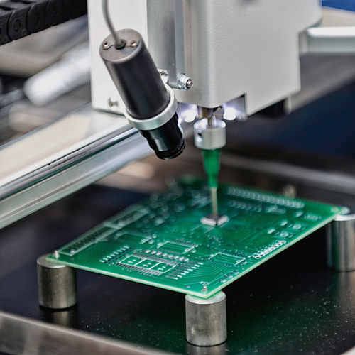
Surface Mount Technology (SMT) has become the industry standard due to its efficiency and versatility. SMT involves mounting electronic components directly onto the surface of printed circuit boards (PCBs). This method significantly enhances the automation potential, allowing for high-speed production and reduced labor costs. The compact nature of SMT components enables the design of smaller and lighter devices, a crucial factor in modern electronics where space and weight are at a premium.

One of the key benefits of SMT is its superior performance in high-frequency applications. The reduced lead length in SMT components minimizes the parasitic inductance and capacitance, leading to better signal integrity and faster operational speeds. This makes SMT the preferred choice for complex and high-speed circuits commonly found in telecommunications, computing, and consumer electronics.

However, SMT is not without its challenges. The smaller component size can make manual handling and inspection difficult, necessitating advanced automated inspection systems. Additionally, SMT components are generally less robust in terms of mechanical strength compared to their through-hole counterparts, which can be a consideration in applications subject to high mechanical stress.

On the other hand, Through-Hole Technology has been a staple in the industry for decades. This method involves inserting component leads through pre-drilled holes in the PCB and soldering them on the opposite side. The primary advantage of through-hole technology is its mechanical stability. The strong solder joints created by this method are highly reliable, making it ideal for applications where durability and longevity are paramount.

Through-hole technology also excels in high-power and high-voltage applications. The robust nature of the components allows them to handle greater electrical currents, making through-hole technology indispensable in industries such as automotive, aerospace, and industrial equipment. Additionally, through-hole components are easier to handle and inspect manually, which can be beneficial for prototyping and low-volume production.

Despite its strengths, through-hole technology has its limitations. The manual insertion process is labor-intensive and time-consuming, leading to higher production costs and longer assembly times. The requirement for drilled holes also reduces the available space on the PCB for routing signals, potentially limiting design flexibility and increasing the board size.

In conclusion, the choice between SMT and through-hole technology depends on the specific requirements of your project. For high-speed, high-density, and cost-sensitive applications, SMT offers unparalleled advantages. Conversely, for high-reliability, high-power, and mechanically robust applications, through-hole technology remains a superior choice. Understanding the pros and cons of each method allows manufacturers to make informed decisions that align with their production goals and application needs.

For more detailed information on our SMT assembly services, visit our Surface Mount Technology Assembly page. Explore how we can help you leverage the strengths of SMT to achieve your project objectives.

What Does It Mean to Be a Full-Service PCB Assembly Provider?

If you are in need of fully assembled printed circuit boards (PCBs) for your products, but you don’t know where to start, this article will guide you in the right direction. If  you don’t have any printed circuit boards or any of the parts, and you certainly don’t want to burden your limited staff with the task of putting all those PCBs together, you will need a full-service PCB assembly provider.

Printed Circuit Board FabricationACME PCB Assembly is an ISO 9001:2015 certified EMS. We make sure you get best price with highest quality, on time delivery schedule. All PCBs are meet the high standards established by the IPC 600. Since ACME PCB Assembly is a IPC certified trainer for IPC A-610, we know how important the quality of bare board is, and we know what can drive the PCB Assembly labor higher.

Being a full-service PCB assembly provider means that we handle every aspect of the project. You just give us your specs, and we’ll do everything else, including:

At Acme PCB Assembly, we have the experience, the vendor relationships, and the well-trained staff of fulfill your PCB order. The great thing about full-service PCB assembly is that you don’t have to worry about a thing. You don’t have to find the right parts vendors or ship materials to us. We handle everything.

We closely match new incoming inquiries to board house equipment and capabilities, ensuring you receive only those inquiries that you are interested in Acme Circuit board assembly provide PCB fabrication service in the development and manufacturing of quality single, double sided and Multi-Layers printed circuit boards for the computer, medical, transportation, communication, aircraft, aerospace and related industries.

Of course, if you already have printed circuit boards on hand and the PCB components you need, then you can also opt for partial service.

Contact us today to learn about all of our service options, including our add-on services.


PCB Fabrication and Assembly

Understanding the PCB Manufacturing Process: From Design to Production

PCB Fabrication near me
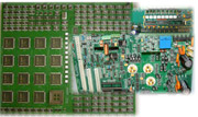
Printed Circuit Boards (PCBs) are the backbone of modern electronics, found in everything from smartphones to medical devices.

At Board Assembly, we pride ourselves on our comprehensive PCB manufacturing process, which ensures top-quality products for a wide range of industries. In this blog, we’ll walk you through the PCB manufacturing process, from initial design to the final product.

1. Design and Layout

The PCB manufacturing journey begins with the design phase. Engineers use specialized software to create a detailed layout of the circuit. This design includes the placement of components, electrical connections, and layer configuration. Ensuring a robust design is crucial as it sets the foundation for the entire manufacturing process.

Key Steps in Design:

  • Schematic Capture: Creating a schematic diagram to represent the circuit.
  • Layout Design: Using CAD software to design the PCB layout.
  • Design Rule Check (DRC): Ensuring the design meets manufacturing specifications.

For more details on our design capabilities, visit our PCB Design Services.

2. Prototyping

Once the design is finalized, a prototype is created. Prototyping is essential to test the design for functionality and performance before mass production. At Board Assembly, we utilize advanced prototyping techniques to ensure quick and accurate results.

Prototyping Steps:

  • Material Selection: Choosing the appropriate materials for the PCB.
  • Initial Fabrication: Creating a small batch of PCBs for testing.
  • Testing and Validation: Conducting thorough tests to verify the design.

Explore our Prototyping Services to learn how we can assist in bringing your designs to life.

3. Material Procurement

The next phase involves procuring the necessary materials. This includes the substrate, copper cladding, and various components like resistors, capacitors, and ICs. Quality materials are vital for the reliability and longevity of the PCB.

Considerations in Material Procurement:

  • Component Quality: Sourcing high-quality components from reputable suppliers.
  • Supply Chain Management: Ensuring timely delivery of materials.
  • Cost Management: Balancing quality with cost-effectiveness.

Find out more about our Material Procurement Process.

4. PCB Fabrication

PCB fabrication is where the actual manufacturing begins. This process involves several steps to transform the design into a physical PCB.

Fabrication Steps:

  • Etching: Removing excess copper to create the circuit pattern.
  • Lamination: Stacking and bonding multiple layers of the PCB.
  • Drilling: Creating holes for component leads and vias.
  • Plating: Adding a layer of conductive material to the drilled holes.

Learn about our PCB Fabrication Techniques for a detailed overview.

5. Assembly

After fabrication, the PCB moves to the assembly phase. This is where components are placed and soldered onto the board.

Assembly Methods:

Discover our PCB Assembly Services to see how we ensure precision and reliability.

6. Testing and Quality Control

Quality control is a critical step to ensure the final product meets all specifications and performance criteria. At Board Assembly, we perform rigorous testing and inspection.

Testing Techniques:

  • Automated Optical Inspection (AOI): Using cameras to inspect the PCB.
  • X-Ray Inspection: Checking for hidden defects.
  • Functional Testing: Ensuring the PCB performs as intended.

Visit our Quality Control Process page to learn more about our commitment to excellence.

7. Final Product and Delivery

Once the PCBs pass all tests, they are ready for delivery. We ensure that each board is packaged securely and delivered on time to our clients.

Delivery Considerations:

Learn more about our Delivery and Support Services.

The PCB manufacturing process is complex and requires meticulous attention to detail at every stage. At Board Assembly, we are dedicated to delivering high-quality PCBs that meet your specific requirements. Whether you need design assistance, prototyping, or full-scale production, we have the expertise and technology to bring your projects to life.

For more information on our services, contact us and let us help you with your next PCB project.

Turnkey Yun Industrial

Differences Between Full Turn Key and Partial Turn Key Printed Circuit Board Services

Differences Between Full Turn Key and Partial Turn Key Printed Circuit Board Services

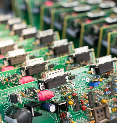
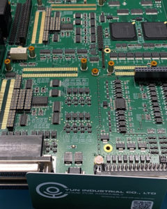
You are looking for a printed circuit board turn-key assembly provider for a new product. When you call up a printed circuit board manufacturer, the first question you are likely to get is, “Do you want full turn key service or partial turn key service?” What is the difference between full and partial turn key service, and what is the best option for you?

Partial Turn Key Service

To make a printed circuit board, the manufacturer needs a variety of components. First, they need the circuit board itself. Next, they’ll need electronic components, conductive tracks, and pads. They may also need capacitors, resistors, and other components that will be soldered onto the printed circuit board.

If you choose partial turn key service, you will be expected to supply your printed circuit board turn-key assembly with the circuit boards along with some of the parts. Your vendor can then get the rest of the parts and proceed with the fabrication of the fully printed circuit board.

The partial turn key option is ideal if you already have a lot of parts on hand and want to save time and money. If you don’t have parts, don’t know where to order the right parts, or don’t even know what the right parts are for your printed circuit board, then the full turn key service is probably a better option for you.

Full Turn Key Service

Turnkey PCB
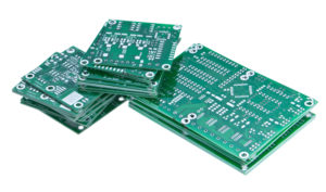
The full turn key service is just like what it sounds. The printed circuit board turn-key assembly provider does all the work. They provide the circuit boards, order all the parts, and fabricate the circuit order. Basically, all you need to do is put in the order. The PCB assembly provider might even be able to help you develop the necessary plans and parts list to get your project off the ground. While a full turn key service will be more expensive than partial turn key service, it can save you a lot of hassle and headaches, especially if you are new to the world of printed circuit boards.

At ACME PCB Assembly, we offer both partial turn key service and full turn key service. We are happy to work with clients from step one of their project or to jump in to complete the project if necessary. If you aren’t sure which service is right for you, contact us today and we would be glad to tell you more about both options.

Our turn-key assembly project for electronics manufacturing services (EMS) model encompasses a broad range of electronics manufacturing services, from design to prototype to production to order fulfillment. We also perform Turn-Key box build, mechanical and final assembly, and packaging.


Restriction of Hazardous Substances (RoHS) Directive

Perhaps the greatest reliability issue to come out of the Restriction of Hazardous Substances (RoHS) Directive is tin whiskers. This residual effect of RoHS is nothing new to electronics manufacturing. Tin whiskers were first been reported in the 1940s and credited with taking down satellites and military planes, causing critical failures to pacemakers and space shuttle systems and even the shutdown of a nuclear power facility.

Tin whiskers cause their fair share of headaches, but they can’t be solved by keeping them out of water and not feeding them after dark. Tin whiskers, their causes and how to prevent them, typically bring more questions than answers. These are the answers Dr. Werner Hügel, Robert Bosch GmbH, has been seeking for years and will discuss during his presentation, “Whisker Prevention and the Relevance of Plating Conditions” during the CALCE Annual Tin Whiskers Symposium at IPC TechSummit, October 28-30, 2014 in Raleigh, N.C.

Dr. Hügel is responsible for the backend technology, galvanic surface finishes and solderability requirements for the automotive electronics division at Robert Bosch. The electronic packages his group is responsible for are found in such areas as: airbag, engine management and transmission control systems, all of which ensure driver and passenger safety. High reliability and low failure rates—especially those caused by tin whiskers—are essential. An electronic short to one of these systems could result in potential harm to people or costly recalls.
Hügel will discuss: four basic whisker growth mechanisms, the relevance of the properties of the tin-finish on whisker formation and whisker mitigation. He will also share insights and data on the influence of plating conditions and plating parameters on whisker performance. Attendees will also learn an approach for effective whisker prevention supported by a modified testing procedure.

The following is a preview of the data, findings and recommendations Hügel will share.

Why whiskers grow

Why tin whiskers grow is a question that has boggled minds for decades. Hügel, however, does have his own theories—on tin whisker formation. According to him, whiskers will grow if there is an overall compressive stress (close to the yield limit of tin) in combination with a stress gradient (- 50 MPa/µm) toward the surface. This situation can be achieved by four basic mechanisms:

•       Growth of irregular intermetallic compounds (IMC) between Cu and Sn
•       Mismatch of coefficient of thermal expansion (CTE) between the base material and tin plating (e.g., delta CTE > 8 ppm)
•       External mechanical force on the tin layer over a long period of time (in press-fit, clamping) not bending
•       Corrosion-induced whisker growth (humid environment)
Why tin finish properties are important
Whisker growth can compromise the functionality of applications; therefore, the risk due to whisker growth has to be minimized, so it’s understandable why tin finish properties themselves are so important. Hügel indicates that tin finish properties are highly relevant to tin whisker growth in terms of:
•       Tin plating process (preparation)
•       Process parameters (process window) (temperature, concentration, agitation, current density, etc.)
•       Electrolyte (type)
•       Maintenance (process conditions such as agitation and current density)
•       Texture of the plating and the robustness of the texture against variations of current density, agitation, etc. The texture itself is the relevant factor regarding whisker growth of the tin plating (impact on CTE, chemical potential, etc.)
Minimizing risk
To minimize the risk of whisker growth, the root cause of whisker growth has to be identified and countermeasures have to be implemented.
According Hügel, “Conformal coating is not seen as the mitigation strategy because of the different side effects and the effectiveness of the coating in case of whisker growth. Third-generation electrolytes can provide excellent performance if the process is well defined and maintained.”
This only scratches the surface of the many parameters that go into whisker formation and prevention. Hügel will delve even deeper into these topics and others.
He will explain why maintenance is a major critical point for tin plating and the necessity for tin plating layer systems to fulfill minimum requirements (thickness, plating system setup, type of plating). He will also share how, by arming yourself with the knowledge of the robustness of the plating, a no-whisker, tin plating can be achieved.
For more information on the CALCE Annual Tin Whiskers Symposium at IPC TechSummit 2014, and to register, go to www.ipc.org/TechSummit.