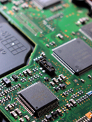
As environmental regulations continue to tighten around the world, lead-free assembly has become an essential requirement in modern electronics manufacturing. Traditional soldering methods often relied on lead-based materials, which are now restricted under global environmental regulations such as the RoHS (Restriction of Hazardous Substances) Directive. Lead-free PCB assembly eliminates hazardous lead from the manufacturing process while maintaining the high mechanical strength and electrical conductivity required for reliable electronic performance.
 At Board Assembly, lead-free assembly processes are designed to meet strict international compliance standards while maintaining the performance and durability expected in high-quality electronics. Using advanced reflow soldering profiles and specialized lead-free solder alloys, the manufacturing process ensures strong solder joints that withstand thermal stress, vibration, and long-term use. These modern soldering techniques provide the reliability needed for demanding electronic applications while supporting environmentally responsible manufacturing practices.
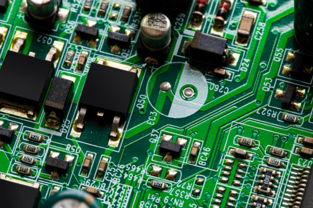
Lead-free PCB assembly requires a higher level of precision compared to traditional lead-based soldering. Lead-free solder alloys typically melt at higher temperatures, which means the reflow process must be carefully controlled to protect sensitive electronic components. Accurate temperature management, precise solder paste application, and strict process monitoring are critical to achieving consistent results. Because of these factors, lead-free assembly often involves tighter manufacturing tolerances and more advanced inspection procedures to ensure quality.
Advanced quality control methods are used throughout the lead-free assembly process to verify proper solder joint formation and component placement. Automated Optical Inspection (AOI), X-ray inspection, and electrical testing help identify potential defects and confirm that every PCB meets rigorous performance standards. These inspection procedures are especially important for high-density circuit boards and complex multilayer designs used in modern electronic products.
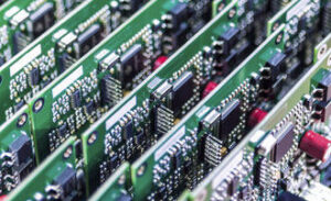
When lead-free assembly is integrated with SMT assembly and PCB fabrication services, manufacturers benefit from a seamless production process that maintains compliance throughout the entire electronics manufacturing cycle. Working with a single provider helps reduce communication errors between suppliers, shortens production timelines, and ensures that environmental and quality standards are consistently maintained from the initial PCB fabrication stage through final assembly and testing.
Benefits of lead-free assembly include:
-
RoHS compliance for global electronics markets
-
Environmentally responsible manufacturing practices
-
Improved access to international markets with strict environmental regulations
-
Reduced exposure to toxic materials during manufacturing and product use
-
Long-term product reliability and durability
Electronics manufacturers that export products internationally must comply with strict environmental directives across multiple regions. Lead-free assembly ensures that products meet these requirements while maintaining the performance standards expected in industries such as aerospace, automotive, telecommunications, and medical devices. Compliance not only protects the environment but also helps companies avoid costly regulatory issues and product restrictions.
Partnering with a full-service electronics manufacturing provider simplifies the compliance process. By combining PCB fabrication, SMT assembly, testing, and conformal coating services, Board Assembly offers end-to-end manufacturing solutions designed to meet modern environmental standards while delivering the quality and reliability required for high-performance electronics.
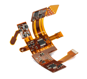
 The heat allows for simple flow of the adhesive which is needed because it must fill-in any and all gaps among the traces and pads to stop the trapping of air between layers. To a flex turnkey PCB assembly designer this means the cover lay openings for a characteristic 1 oz. The copper plan must be out-sized by 10 mils, which is appreciably bigger than the typical huge of 2-3 mils used on conventional PCB solder masks.
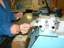
 For a long time, lead has been part of the soldering process, which is critical to making printed circuit boards. Here at


