ACME PCB Assembly: A Greenhouse for Sustainable Electronic Manufacturing
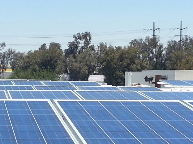
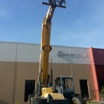
 ACME PCB Assembly is setting a remarkable example of sustainability in electronic manufacturing by leveraging renewable energy. Their solar panel system, which generates 64.2KW, offers incredible environmental benefits. Over the next 30 years, this PV system is projected to offset 4,136,092 pounds of CO2 emissions, reduce particulates linked to asthma by 817 pounds, and equate to taking 21.8 cars off the road for 25 years or planting 35.5 acres of trees. Impressive, isn’t it? A well-deserved round of applause for ACME PCB Assembly!
The drive to “go green” stems from more than just a desire to conserve nature. It’s about fostering economic growth, ensuring social and physical well-being, and securing a sustainable future. As industries like electronics heavily rely on natural resources, the shift to eco-conscious practices is both necessary and urgent.
According to EcoWatch, the depletion of resources vital to powering economies and improving livelihoods is an escalating environmental and economic concern. Non-renewable materials, essential for many industries, are being exhausted at alarming rates. Even renewable resources face challenges, as their replenishment often requires significant time. The experts emphasize the pressing need for industries to adopt sustainable strategies to mitigate these risks.
Why Sustainability Matters
The electronics industry relies heavily on natural resources, making the shift to sustainable practices both urgent and necessary. According to environmental experts, the depletion of non-renewable resources is accelerating, while even renewable resources require significant time to replenish. Without action, industries risk exhausting the materials vital to powering economies and improving livelihoods.
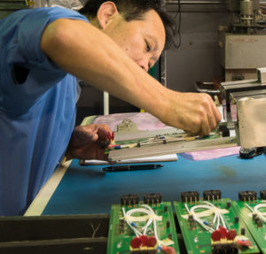
At ACME PCB Assembly, we recognize this challenge and are taking proactive steps to address it. By adopting green manufacturing practices, we’re not only conserving resources but also inspiring others to follow suit.
Join the Green Revolution
Sustainability is the future of manufacturing, and ACME PCB Assembly is leading the way. By leveraging renewable energy and eco-friendly processes, we’re proving that innovation and environmental responsibility go hand in hand.
Learn more about how we’re transforming electronic manufacturing at ACME PCB Assembly. Together, we can build a greener, more sustainable future.
At ACME PCB Assembly, sustainability is not just a buzzword—it’s an operational standard. By integrating green practices into their processes, they are not only reducing their ecological footprint but also inspiring others to follow suit.
Curious to learn more about how ACME PCB Assembly is leading the way in green electronic manufacturing? Contact us today and discover how sustainability can power innovation.
Contact us for more information how we go green in our processes.

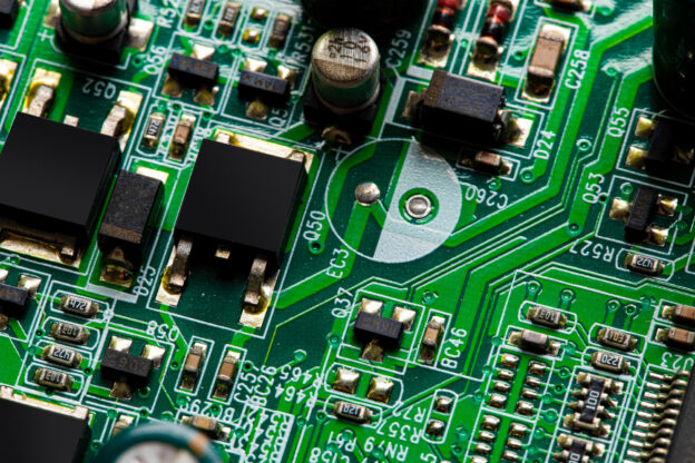
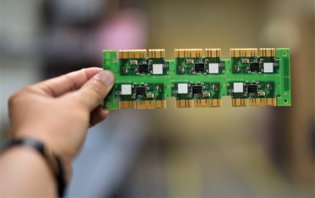
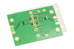 One of the most important steps in bringing any new electronic device to market is completing the prototype phase. A prototype doesn’t just prove that your idea can work; it becomes the foundation for improving your design, testing functionality, pitching investors, and preparing for manufacturing. At ACME PCB Assembly, we specialize in helping inventors, entrepreneurs, and start-ups build the printed circuit boards (PCBs) their products depend on.