The world of printed circuit board (PCB) technology is evolving rapidly. As design demands grow denser, smarter, and more compact, three trends are defining the next generation of electronics: High-Density Interconnect (HDI), Flexible & Rigid-Flex PCBs, and Embedded Components. At Board Assembly, we’re keeping a close eye on these advances to ensure our clients stay ahead of the curve.
1. HDI: Packing More into Less
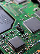
HDI technology enables PCBs with tighter trace spacing, smaller vias, buried and blind vias, and multiple layers of interconnects. These capabilities support miniaturization while maintaining signal integrity. In fact, Ultra-HDI is pushing the envelope even further, with features like microvias smaller than 2 mil and dense layer stacking becoming more commonplace in 2025.
For applications in high-speed communication, computing, and mobile devices, HDI is indispensable. It allows more functionality per square millimeter and reduces signal path length, which helps with high-frequency performance.
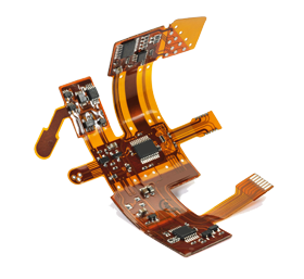
2. Flexible & Rigid-Flex PCBs: Form Meets Function
Rigid-flex and flexible PCBs bridge the gap between rigid boards and adaptable electronics. As IoT, wearables, and foldable electronics grow in importance, demand for flexible interconnects is rising sharply.
These flexible circuits allow boards to bend, fold, or conform to shapes, reducing connector count, saving space, and improving reliability. Designers are combining rigid and flex segments into single boards (rigid-flex) to gain mechanical stability where needed and flexibility where required.
In 2025, we’re seeing material innovations: thinner substrates, more durable flex films, and improved adhesion layers, all designed to survive repeated bending cycles and harsh environmental conditions.
3. Embedded Components: The Next Level of Integration
Embedded component technology involves placing passive and sometimes active devices (resistors, capacitors, ICs) within the layers or substrate of a PCB rather than on its surface. This approach reduces board surface complexity, shrinks form factors, and improves performance by shortening signal paths.
By embedding components, PCB designers can reduce external solder joints, minimize parasitic inductance, and better manage circuit density. This trend is especially relevant for compact, performance-sensitive sectors like aerospace, medical devices, and wearable electronics.
 Why These Trends Matter for Your Projects
-
Smaller form factors: More capability in less space.
-
Better performance: Shorter interconnects, cleaner signal paths, less noise.
-
Reliability & durability: Fewer external interconnects, more mechanically robust designs.
-
Modern applications: These technologies enable cutting-edge devices in AI, 5G, IoT, and more.
At Board Assembly, we support HDI, flexible, rigid-flex, and embedded-component assemblies to meet the demands of tomorrow’s electronics. Whether you’re prototyping or producing in volume, we’re ready to partner with you.


