Tag Archives: electronics miniaturization

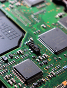
2 BGAs or More vertical installing.

The Rise of Package on Package (PoP) in PCB Assembly

In the ever-evolving landscape of electronics manufacturing, Package on Package (PoP) technology is transforming how circuit boards are designed and assembled. First gaining traction in the early 2000s, PoP is now considered one of the most innovative advances since the introduction of Ball Grid Array (BGA) components in the mid-1990s.

At its core, PoP is an integrated circuit packaging method that vertically stacks two or more BGA packages—typically combining a logic processor and memory component. This space-saving configuration allows for compact, high-performance assemblies ideal for smartphones, wearables, medical devices, and advanced industrial electronics.

The Advantages of PoP Technology

The primary benefit of PoP technology lies in its ability to reduce external pin count through package-level system integration. By stacking chips vertically, engineers can achieve a smaller footprint without sacrificing power or performance. This simplification not only optimizes PCB layout efficiency but also improves overall product reliability by minimizing interconnect lengths and signal interference.

Depending on the configuration, PoP packages can reach a total height as low as 1.4mm, making them perfect for compact devices where every millimeter counts. Additionally, PoP assemblies support independent testing of logic and memory layers, resulting in higher manufacturing yields and easier defect isolation during production.

ACME PCB Assembly: Leading the Way Since 2009

Since 2009, ACME PCB Assembly has been a leader in adopting and refining PoP technology. Utilizing advanced FUJI assembly lines and precise reflow soldering techniques, ACME delivers reliable PoP BGA assemblies for both prototype runs and medium-batch production.

From single-unit builds to production runs of up to 20,000 pieces, ACME’s skilled technicians ensure precise alignment, solder integrity, and quality control at every stage. This allows clients to seamlessly integrate high-density packaging into their next-generation designs—accelerating time to market while maintaining exceptional performance standards.

Whether you’re developing consumer electronics, industrial control systems, or medical devices, PoP technology offers a compact and efficient solution.

Embrace the Future of PCB Assembly

2 BGAs or More vertical installing.

ACME PCB Assembly is your trusted partner for Package on Package assembly, offering experience, precision, and scalability for your most advanced designs. Contact Board Assembly today at 310-715-1898 to learn how PoP can enhance your next project.

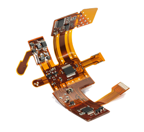
Flexible Circuit board

Trends in PCB Technology 2025: HDI, Flexible PCBs & Embedded Components

The world of printed circuit board (PCB) technology is evolving rapidly. As design demands grow denser, smarter, and more compact, three trends are defining the next generation of electronics: High-Density Interconnect (HDI), Flexible & Rigid-Flex PCBs, and Embedded Components. At Board Assembly, we’re keeping a close eye on these advances to ensure our clients stay ahead of the curve.

1. HDI: Packing More into Less

HDI technology enables PCBs with tighter trace spacing, smaller vias, buried and blind vias, and multiple layers of interconnects. These capabilities support miniaturization while maintaining signal integrity. In fact, Ultra-HDI is pushing the envelope even further, with features like microvias smaller than 2 mil and dense layer stacking becoming more commonplace in 2025.

For applications in high-speed communication, computing, and mobile devices, HDI is indispensable. It allows more functionality per square millimeter and reduces signal path length, which helps with high-frequency performance.

2. Flexible & Rigid-Flex PCBs: Form Meets Function

Rigid-flex and flexible PCBs bridge the gap between rigid boards and adaptable electronics. As IoT, wearables, and foldable electronics grow in importance, demand for flexible interconnects is rising sharply.

These flexible circuits allow boards to bend, fold, or conform to shapes, reducing connector count, saving space, and improving reliability. Designers are combining rigid and flex segments into single boards (rigid-flex) to gain mechanical stability where needed and flexibility where required.

In 2025, we’re seeing material innovations: thinner substrates, more durable flex films, and improved adhesion layers, all designed to survive repeated bending cycles and harsh environmental conditions.

3. Embedded Components: The Next Level of Integration

Embedded component technology involves placing passive and sometimes active devices (resistors, capacitors, ICs) within the layers or substrate of a PCB rather than on its surface. This approach reduces board surface complexity, shrinks form factors, and improves performance by shortening signal paths.

By embedding components, PCB designers can reduce external solder joints, minimize parasitic inductance, and better manage circuit density. This trend is especially relevant for compact, performance-sensitive sectors like aerospace, medical devices, and wearable electronics.


Printed Circuit Board FabricationWhy These Trends Matter for Your Projects

  • Smaller form factors: More capability in less space.

  • Better performance: Shorter interconnects, cleaner signal paths, less noise.

  • Reliability & durability: Fewer external interconnects, more mechanically robust designs.

  • Modern applications: These technologies enable cutting-edge devices in AI, 5G, IoT, and more.

At Board Assembly, we support HDI, flexible, rigid-flex, and embedded-component assemblies to meet the demands of tomorrow’s electronics. Whether you’re prototyping or producing in volume, we’re ready to partner with you.