When it comes to electronic products, the materials you choose for your printed circuit board (PCB) can make all the difference in performance, reliability, and even cost. Selecting the right PCB material isn’t just about picking what’s readily available; it’s about matching the material’s properties to your specific application. At Board Assembly, we understand the importance of PCB material selection and are here to help you navigate the options.
Why PCB Material Matters
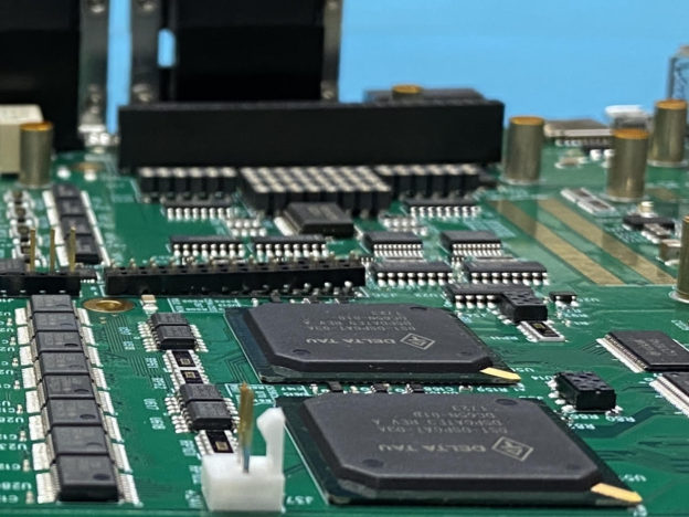
Your PCB is the backbone of your electronic device. It carries electrical signals, manages heat, and supports all your components. The wrong material choice can lead to issues like signal loss, overheating, or even mechanical failure. That’s why understanding your project’s requirements is key to making the right choice.
Factors to Consider
-
 Thermal Performance:
If your application generates a lot of heat—like in power electronics or LED lighting—you’ll need a PCB material with good thermal conductivity. Materials like aluminum-based PCBs or high-Tg FR-4 are excellent choices. -
Electrical Performance:
For high-frequency or RF applications, you’ll need a material with low dielectric loss. PTFE-based materials are often recommended for their superior electrical properties. -
Mechanical Strength:
Will your PCB be exposed to vibrations, shock, or mechanical stress? If so, choose materials with higher mechanical strength to avoid cracks and failures. -
Cost:
Budget matters too. While advanced materials like Rogers or ceramic substrates offer excellent performance, they can be pricey. For many applications, standard FR-4 remains a reliable and cost-effective option. -
Environmental Conditions:
Consider the environment your PCB will operate in. Will it face moisture, chemicals, or extreme temperatures? Some materials offer better resistance to harsh conditions.
Trust Board Assembly with Your PCB Needs
At Board Assembly, we guide our customers through every step of the PCB material selection process. Our team helps you find the perfect balance between performance and budget, ensuring your project is a success.
📞 Contact us today to learn more about our services and how we can help you choose the best PCB material for your application.
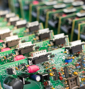
 BGA assembly is a type of SMT process, which is used for
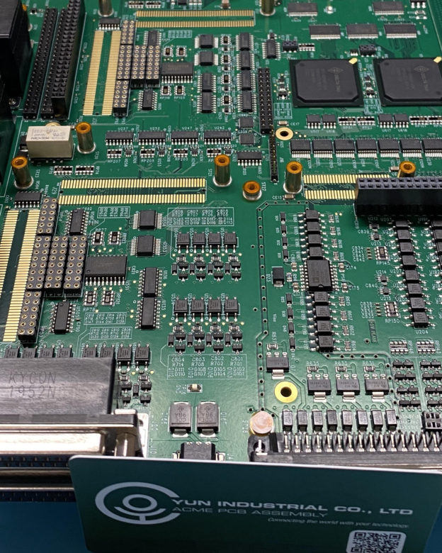
 What Is Turnkey Printed Circuit Board Assembly?
 The ACME PCB Assembly Advantage
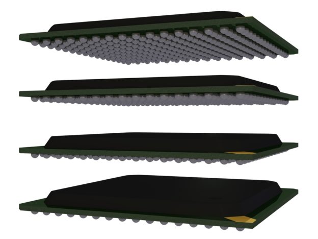
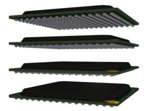
 There are two popular configurations for PoP assemblies:
 PRINTED CIRCUIT BOARD ASSEMBLY COMPANY TO MEET YOUR DEADLINES


