In the world of printed circuit board (PCB) manufacturing, thru-hole assembly services remain a critical choice for projects demanding strength, durability, and reliability. While surface mount technology (SMT) often dominates discussions about electronics assembly, thru-hole assembly has unique benefits that make it indispensable for certain applications — especially in industrial, aerospace, automotive, and defense systems where component permanence and mechanical integrity are essential.
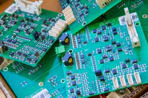 Thru-hole assembly involves inserting electronic component leads into drilled holes on a PCB and soldering them in place. This process creates mechanically robust solder joints, superior to many surface mount options when it comes to withstanding vibration and thermal stress. Industries that demand long-life performance and high reliability often favor thru-hole components like connectors, large capacitors, transformers, and tall leaded components that simply cannot be mounted using SMT alone.
Choosing an expert provider of thru-hole assembly ensures consistent quality and performance. BoardAssembly’s dedicated team specializes in integrating thru-hole techniques with modern manufacturing controls, delivering assemblies that meet stringent quality standards. Whether your project requires selective soldering, manual insertion, or hybrid assembly workflows, a trusted partner with experience across technologies is vital.
One major advantage of thru-hole assembly is its compatibility with automated wave soldering — a highly efficient soldering process for large volumes of boards with thru-hole components. When paired with thorough inspection and process controls, wave soldering enhances throughput while maintaining consistency.
Despite its strengths, thru-hole assembly is often used alongside SMT in a mixed technology assembly environment. Most advanced electronic systems leverage both technologies: SMT for dense, fine-pitch parts and thru-hole for components requiring solid mechanical support. BoardAssembly understands how to balance these techniques within a single PCB assembly workflow to optimize performance and cost.
To further support complete electronics manufacturing solutions, BoardAssembly also offers comprehensive services including EMS (Electronic Manufacturing Services) and turnkey assembly, creating seamless results from prototype to full production. By combining expert thru-hole assembly with strategic manufacturing planning, customers gain faster time to market and fewer production delays.
For designers and engineers, early collaboration with your assembly partner on DFM (Design for Manufacturability) feedback is essential. Proactive analysis during the design phase reduces risks and ensures that thru-hole components are placed and oriented for efficient assembly and long-term functionality.
In summary, thru-hole assembly remains a valuable and relevant process within modern PCB production — especially when executed by experienced professionals with access to advanced tools and quality systems. Integrating thru-hole services into your next PCB build can enhance strength, reliability, and overall product performance.
Learn more about industry-leading thru-hole assembly services at https://boardassembly.com/thru-hole-assembly/.

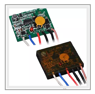
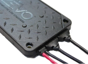 Industries that rely heavily on these services include automotive electronics, outdoor communication systems, aerospace and defense equipment, marine technology, renewable energy systems, and rugged industrial controls. Any application exposed to environmental hazards can benefit from the long-term reliability provided by professional potting and encapsulation.
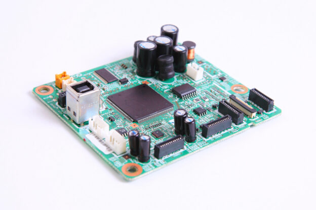
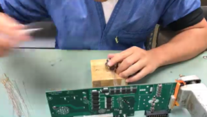 Beyond mechanical assembly, Board Assembly also provides a full suite of value-added electronic services. These include firmware loading, software installation, device programming, calibration, and functional verification. Each unit undergoes thorough testing based on customer requirements—ranging from continuity checks and LED verification to complete system-level operational tests. This ensures the finished product is fully functional and deployment-ready upon delivery.
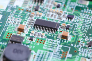 Our process begins with thorough PCB cleaning, ensuring no contaminants interfere with adhesion. Depending on the project, we apply coatings using automated selective coating systems, brushing, spraying, or dipping. Complex assemblies with connectors, switches, or areas requiring masking are handled precisely, preventing material from covering critical contact points.
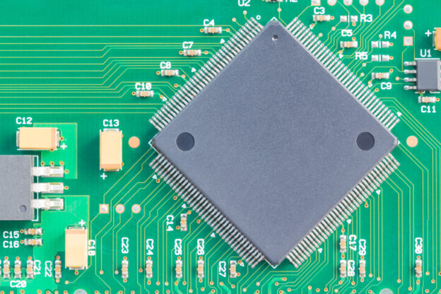
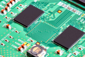 Once the assembly begins, solder paste is applied using tightly controlled stencil printing methods. This ensures proper solder volume, which is critical for component adhesion and long-term performance. Our automated reflow ovens use multi-zone temperature profiling to ensure consistent solder joints across every PCB. Whether your project requires leaded or RoHS-compliant lead-free soldering, Board Assembly adheres to strict temperature controls that guarantee reliability.


