Tag Archives: printed circuit boards usa

Printed Circuit Board Fabrication

Is it Possible to Recycle Your Unused Printed Circuit Boards?

We will be discussing the issue of PCB recycling, if it’s even possible, how it is done and what can we do as electronics design engineers to create more recyclable PCBs. When we say PCB we are meaning a PCB without any components on it.  Most electronic devices found out there have their components sitting in a nice looking Printed Circuit Board or PCB.  Since electronic devices are in high demand, PCBs are everywhere. Making sure their materials can be collected and reused instead of just throwing them into a landfill would potentially be a smart and environmentally sensible move if performed properly.

Remember that large order of printed circuit boards you ordered? You thought it would be a good idea to have a surplus of parts on hand in case you needed to increase production of your product line. Unfortunately, that product got discontinued, so now you have a huge stash of PCBs taking up room in your warehouse and on your accounting books. It is time to trash them?

Not so fast! In many cases, printed circuit boards can be reworked and modified. Do you have another electronic or computerized product in the works? Then contact ACME PCB Assembly  we may be able to re-purpose your PCBs. Our workers are highly trained in de-soldering and re-soldering surface mounted electronic components. We have also invested in specialized equipment that can assist us in these efforts.

Can you recycle your old PCB?

Yes and no, before coming to a final decision let’s first see what a PCB is made of. A PCB is basically a layered sandwich of copper and FR-4. FR-4 is a fiberglass with an epoxy resin that has the purpose of bonding the fiber together and as an adhesive, it is also flame resistant. Apart from that, you can also find tin and small traces of gold and silver.

Don’t throw out unused printed circuit boards.
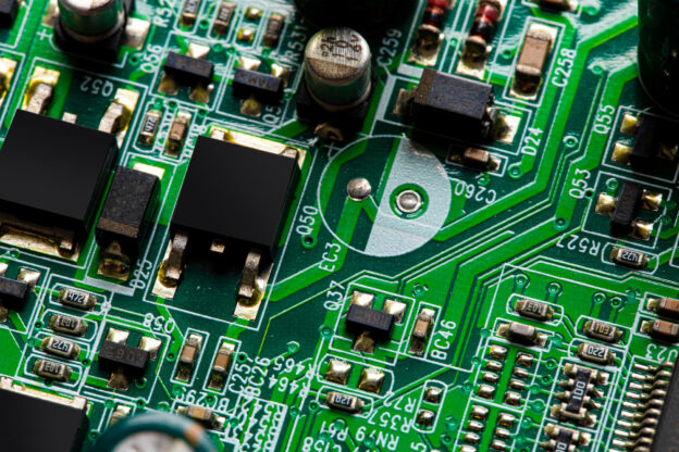
Give us a call today to learn how we could possibly turn them into components for your next big product!

Printed circuit board production

Surface Mount Technology (SMT) vs. Through-Hole Technology: Pros and Cons

In the ever-evolving world of electronics manufacturing, choosing the right assembly method is crucial for optimizing both performance and cost-efficiency. Two prominent techniques in this realm are Surface Mount Technology (SMT) and Through-Hole Technology. Each has its own advantages and drawbacks, making it essential to understand their unique characteristics and applications.

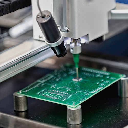
Printed circuit board productionSurface Mount Technology (SMT) has become the industry standard due to its efficiency and versatility. SMT involves mounting electronic components directly onto the surface of printed circuit boards (PCBs). This method significantly enhances the automation potential, allowing for high-speed production and reduced labor costs. The compact nature of SMT components enables the design of smaller and lighter devices, a crucial factor in modern electronics where space and weight are at a premium.

One of the key benefits of SMT is its superior performance in high-frequency applications. The reduced lead length in SMT components minimizes the parasitic inductance and capacitance, leading to better signal integrity and faster operational speeds. This makes SMT the preferred choice for complex and high-speed circuits commonly found in telecommunications, computing, and consumer electronics.

However, SMT is not without its challenges. The smaller component size can make manual handling and inspection difficult, necessitating advanced automated inspection systems. Additionally, SMT components are generally less robust in terms of mechanical strength compared to their through-hole counterparts, which can be a consideration in applications subject to high mechanical stress.

On the other hand, Through-Hole Technology has been a staple in the industry for decades. This method involves inserting component leads through pre-drilled holes in the PCB and soldering them on the opposite side. The primary advantage of through-hole technology is its mechanical stability. The strong solder joints created by this method are highly reliable, making it ideal for applications where durability and longevity are paramount.

Through-hole technology also excels in high-power and high-voltage applications. The robust nature of the components allows them to handle greater electrical currents, making through-hole technology indispensable in industries such as automotive, aerospace, and industrial equipment. Additionally, through-hole components are easier to handle and inspect manually, which can be beneficial for prototyping and low-volume production.

Despite its strengths, through-hole technology has its limitations. The manual insertion process is labor-intensive and time-consuming, leading to higher production costs and longer assembly times. The requirement for drilled holes also reduces the available space on the PCB for routing signals, potentially limiting design flexibility and increasing the board size.

In conclusion, the choice between SMT and through-hole technology depends on the specific requirements of your project. For high-speed, high-density, and cost-sensitive applications, SMT offers unparalleled advantages. Conversely, for high-reliability, high-power, and mechanically robust applications, through-hole technology remains a superior choice. Understanding the pros and cons of each method allows manufacturers to make informed decisions that align with their production goals and application needs.

For more detailed information on our SMT assembly services, visit our Surface Mount Technology Assembly page. Explore how we can help you leverage the strengths of SMT to achieve your project objectives.