Author Archives: Stephen Yun

PCB layout and circuitry design

Circuitry Design: Why Companies Outsource PCB Layout and Design

In today’s electronics market, circuitry design and PCB layout play a critical role in product performance, reliability, and manufacturability. As devices become smaller and more complex, many companies choose to outsource PCB design services rather than manage the process entirely in-house. Outsourcing PCB layout and design is not just a cost decision—it’s a strategic move that improves efficiency, quality, and speed to market.

What Does Outsourcing PCB Design Mean?

Outsourcing can be defined as the strategic use of outside resources to perform specialized tasks more efficiently. When companies outsource PCB layout and circuitry design, they gain access to experienced engineers, advanced design tools, and proven workflows—without the overhead of maintaining an internal design team.

Deciding to outsource PCB design can be straightforward when the right process is followed.

Key Stages in the PCB Design Outsourcing Process

Initial Design Review

The process begins with a detailed discussion between your design engineer and the PCB layout specialist. During this stage, requirements such as electrical specifications, signal integrity needs, power constraints, compliance standards, and manufacturing goals are clearly defined. A strong initial design review reduces revisions and ensures the PCB design aligns with your product objectives from the start.

Mechanical Review

Mechanical definition is essential before any components are placed. This stage focuses on creating the board outline and confirming physical constraints. Important considerations include tool holes, break-away panels, fiducial marks, mounting points, and overall product dimensions. Providing enclosure drawings and mechanical specifications ensures the PCB fits seamlessly into the final product and meets all mechanical requirements.

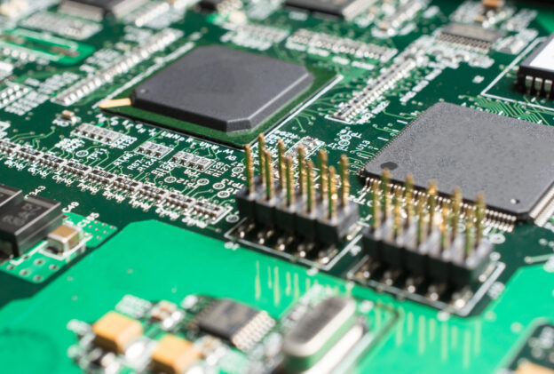
Component Placement and Review

Component placement has a direct impact on assembly cost, performance, and reliability. Poor placement can lead to higher assembly labor, increased failure rates, and long-term reliability issues. An experienced PCB layout provider optimizes component positioning for manufacturability, signal integrity, thermal performance, and efficient assembly—reducing errors and improving yield.

Benefits of Outsourcing PCB Layout and Design

  • Access to experienced PCB design engineers

  • Reduced development time and faster product launches

  • Lower internal engineering and staffing costs

  • Improved design for manufacturability (DFM)

  • Higher quality, lower failure rates, and better long-term reliability

By outsourcing circuitry design, companies can focus on innovation, product development, and core business operations while relying on experts for precision PCB layout.

Partner with Board Assembly for Expert PCB Design

At Board Assembly, we provide professional PCB layout, circuitry design, and manufacturing support to help your products succeed. Our team works closely with your engineers to deliver accurate, manufacturable designs that meet performance and cost goals.

Contact Board Assembly today to discuss your PCB design and layout needs and discover how outsourcing can improve efficiency, quality, and time to market.

Improving PCB Reliability with Advanced X-Ray Inspection for BGA Assembly

In today’s electronics industry, printed circuit boards are becoming smaller, faster, and more complex. As components shrink and circuit density increases, manufacturers must rely on more advanced inspection technologies to ensure every connection performs reliably. At Acme PCB Assembly, maintaining the highest quality standards is a top priority, which is why we utilize advanced X-ray inspection technology to support our manufacturing process.

Hidden solder connections found in components like Ball Grid Arrays (BGAs) cannot be inspected through traditional visual inspection methods. These components require specialized imaging technology to verify the integrity of solder joints beneath the package. Our advanced X-ray inspection capabilities allow our engineering and quality teams to evaluate these internal connections and ensure that every board meets strict reliability requirements.

This technology plays a critical role in our and BGA Board Assembly with X-ray in California services, allowing us to validate complex assemblies used in a wide range of electronic applications.

The Role of X-Ray Inspection in Modern PCB Manufacturing

Standard inspection techniques are effective for many surface-mounted components, but hidden solder joints require deeper analysis. X-ray inspection enables technicians to examine the internal structure of a circuit board without removing components or damaging the assembly.

With high-resolution imaging and multi-angle viewing, our X-ray inspection process helps detect issues such as:

  • Voids inside solder joints
  • Insufficient solder connections
  • Solder bridging between pads
  • Component misalignment
  • Structural defects within the assembly

By identifying these issues early in the manufacturing process, Acme PCB Assembly can correct potential problems before boards move into final production or field use.

Supporting High-Density BGA Board Assembly

BGA Board Assembly offers many advantages, including improved electrical performance, greater connection density, and more compact designs. However, because the solder balls are located underneath the component, verifying the quality of each connection requires advanced inspection techniques.

Our X-ray inspection capabilities provide the level of verification needed to support dependable BGA Assembly production. This is especially important for industries where reliability is critical, including:

  • Medical electronics
  • Aerospace systems
  • Telecommunications equipment
  • Industrial control systems
  • Automotive electronics

By implementing advanced inspection tools within our manufacturing workflow, we ensure every board meets the performance standards required for these demanding applications.

Key Benefits of X-Ray Inspection in PCB Assembly

Incorporating X-ray inspection technology into the manufacturing process provides several important advantages for customers:

  • Improved defect detection before products leave production
  • Consistent inspection standards across complex assemblies
  • Higher reliability for advanced PCB designs
  • Detailed quality data for traceability and documentation
  • Greater confidence in long-term product performance

These capabilities help reduce the risk of product failures and support the delivery of dependable electronic assemblies.

Work with an Experienced BGA Assembly Provider

As electronic designs continue to evolve, manufacturers must rely on advanced inspection technology to verify increasingly complex circuit boards. Acme PCB Assembly combines experienced engineering, precise manufacturing processes, and advanced inspection tools to ensure each product meets the highest standards.

If your project requires precision BGA Board Assembly X-ray inspection in California, our team is ready to support your production needs.

Contact Acme PCB Assembly today to learn how our PCB assembly expertise and advanced inspection capabilities can help ensure the success of your next electronics project.

Strengthening SMT Assembly Quality with Omron 3D AOI S1080

We are proud to announce the addition of the Omron 3D AOI S1080 system to our production line, a major investment dedicated to maintaining and enhancing the highest standards of SMT assembly quality. As electronic products continue to evolve toward miniaturization, higher complexity, and greater reliability requirements, the importance of consistent inspection and process control has never been more critical.

The Omron S1080 represents the latest generation of 3D Automated Optical Inspection (AOI) technology. With advanced 3D imaging, precise height measurement, and intelligent defect detection algorithms, it ensures that every solder joint, component placement, and fine-pitch assembly meets strict quality standards. Unlike traditional 2D AOI, the 3D system eliminates false calls caused by shadows or reflections and provides accurate detection of defects such as insufficient solder, lifted leads, bridging, and coplanarity issues.


By integrating the S1080 directly into our SMT assembly workflow, we gain real-time feedback that allows us to identify potential process variations before they affect product quality. This supports our continuous improvement initiatives, minimizes rework, and reduces costs for our customers. The inspection data collected also enables comprehensive traceability and analytics, giving us the ability to refine our process parameters and further enhance efficiency.


For customers, the addition of Omron’s S1080 means greater confidence in product reliability. Whether the project requires high-mix low-volume builds or high-volume production, this 3D AOI system helps us ensure that each board delivered is manufactured with precision and consistency. Our commitment goes beyond simply meeting industry standards—we aim to exceed them by implementing state-of-the-art tools that safeguard quality at every stage of SMT assembly.


With the Omron 3D AOI S1080 in place, we reaffirm our focus on quality, innovation, and customer satisfaction. This strategic investment reflects our ongoing mission: to provide manufacturing services that combine world-class technology with rigorous quality assurance, ensuring that every product leaving our facility embodies reliability and excellence.